Darlington Transistors
The Darlington Transistor configuration of two bipolar transistors offers increased current switching for a given base current
The Darlington Transistor named after its inventor, Sidney Darlington is a special arrangement of two standard NPN or PNP bipolar junction transistors (BJT) connected together. The Emitter of one transistor is connected to the Base of the other to produce a more sensitive transistor with a much larger current gain being useful in applications where current amplification or switching is required.
Darlington Transistor pairs can be made from two individually connected bipolar transistors or a one single device commercially made in a single package with the standard: Base, Emitter and Collector connecting leads and are available in a wide variety of case styles and voltage (and current) ratings in both NPN and PNP versions.
As we saw in our Transistor as a Switch tutorial, as well as being used as an amplifier, the bipolar junction transistor, (BJT) can be made to operate as an ON-OFF switch as shown.
Bipolar Transistor as a Switch
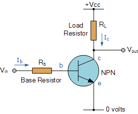
When the base of the NPN transistor is grounded (0 volts) and no base current, Ib flows, no current flows from the emitter to the collector and the transistor is therefore switched “OFF”. If the base is forward biased by more than 0.7 volts, a current will flow from the emitter to the collector and the transistor is said to be switched “ON”. When operated in these two modes, the transistor operates as a switch.
The problem here is that the transistors Base needs to be switched between zero and some large, positive value for the transistor to become saturated at which point an increased base current, Ib flows into the device resulting in collector current Ic becoming large while Vce is small. Then we can see that a small current on the base can control a much larger current flowing between the collector and the emitter. The ratio of collector current to base current ( β ) is known as the current gain of the transistor. A typical value of β for a standard bipolar transistor may be in the range of 50 to 200 and varies even between transistors of the same part number. In some cases where the current gain of a single transistor is too low to directly drive a load, one way to increase the gain is to use a Darlington pair.
A Darlington Transistor configuration, also known as a “Darlington pair” or “super-alpha circuit”, consist of two NPN or PNP transistors connected together so that the emitter current of the first transistor TR1 becomes the base current of the second transistor TR2. Then transistor TR1 is connected as an emitter follower and TR2 as a common emitter amplifier as shown below.
Also note that in this Darlington pair configuration, the collector current of the slave or control transistor, TR1 is “in-phase” with that of the master switching transistor TR2.
Basic Darlington Transistor Configuration
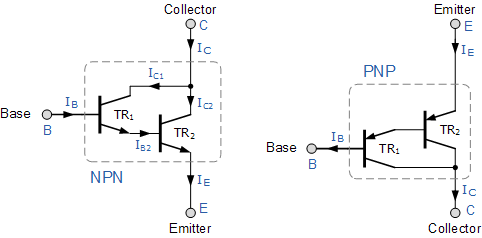
Using the NPN Darlington pair as the example, the collectors of two transistors are connected together, and the emitter of TR1 drives the base of TR2. This configuration achieves β multiplication because for a Base current ib, the collector current is β*ib where the current gain is greater than one, or unity and this is defined as:
But the base current, IB2 is equal to transistor TR1 emitter current, IE1 as the emitter of TR1 is connected to the base of TR2. Therefore:
![]()
Then substituting in the first equation:
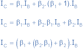
Where β1 and β2 are the gains of the individual transistors.
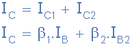
This means that the overall current gain, β is given by the gain of the first transistor multiplied by the gain of the second transistor as the current gains of the two transistors multiply. In other words, a pair of bipolar transistors combined together to make a single Darlington transistor pair can be regarded as a single transistor with a very high value of βand consequently a high input resistance.
Darlington Transistor Example No1
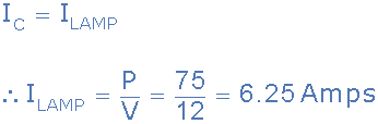
Two NPN transistors are connected together in the form of a Darlington Pair to switch a 12V 75W halogen lamp. If the forward current gain of the first transistor is 25 and the forward current gain (Beta) of the second transistor is 80. Ignoring any voltage drops across the two transistors, calculate the maximum base current required to switch the lamp fully-ON.
Firstly, the current drawn by the lamp will be equal to the Collector current of the second transistor, then:
Using the equation above, the base current is given as:
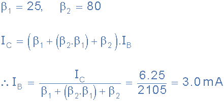
Then we can see that a very small base current of only 3.0mA, such as that supplied by a digital logic gate or the output port of a micro-controller, can be used to switch the 75 Watt lamp “ON” and “OFF”.
If two identical bipolar transistors are used to make a single Darlington device then β1 is equal to β2 and the overall current gain will be given as:
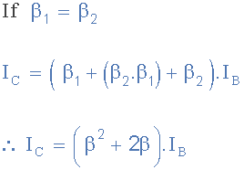
Generally the value of β2 is much greater than that of 2β, in which case it can be ignored to simplify the maths a little. Then the final equation for two identical transistors configured as a Darlington pair can be written as:
Identical Darlington Transistors
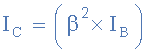
Then we can see that for two identical transistors, β2 is used instead of β acting like one big transistor with a huge amount of gain. Darlington transistor pairs with current gains of more than a thousand with maximum collector currents of several amperes are easily available. For example: the NPN TIP120 and its PNP equivalent the TIP125.
The advantage of using an arrangement such as this, is that the switching transistor is much more sensitive as only a tiny base current is required to switch a much larger load current as the typical gain of a Darlington configuration can be over 1,000 whereas normally a single transistor stage produces a gain of about 50 to 200.
Then we can see that a darlington pair with a gain of 1,000:1, could switch an output current of 1 ampere in the collector-emitter circuit with an input base current of just 1mA. This then makes darlington transistors ideal for interfacing with relays, lamps and motors to low power microcontroller, computer or logic controllers as shown.
Darlington Transistor Applications
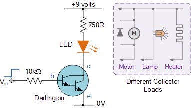
The base of the Darlington transistor is sufficiently sensitive to respond to any small input current from a switch or directly from a TTL or 5V CMOS logic gate. The maximum collector current Ic(max) for any Darlington pair is the same as that for the main switching transistor, TR2 so can be used to operate relays, DC motors, solenoids and lamps, etc.
One of the main disadvantage of a Darlington transistor pair is the minimum voltage drop between the base and emitter when fully saturated. Unlike a single transistor which has a saturated voltage drop of between 0.3v and 0.7v when fully-ON, a Darlington device has twice the base-emitter voltage drop (1.2 V instead of 0.6 V) as the base-emitter voltage drop is the sum of the base-emitter diode drops of the two individual transistors which can be between 0.6v to 1.5v depending on the current through the transistor.
This high base-emitter voltage drop means that the Darlington transistor can get hotter than a normal bipolar transistor for a given load current and therefore requires good heat sinking. Also, Darlington transistors have slower ON-OFF response times as it takes longer for the slave transistor TR1 to turn the master transistor TR2 either fully-ON or fully-OFF.
To overcome the slow response, increased voltage drop and thermal disadvantages of a standard Darlington Transistor device, complementary NPN and PNP transistors can be used in the same cascaded arrangement to produce another type of Darlington transistor called a Sziklai Configuration.