Bipolar Transistor Construction
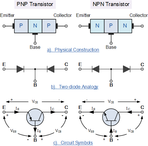
The construction and circuit symbols for both the PNP and NPN bipolar transistor are given above with the arrow in the circuit symbol always showing the direction of “conventional current flow” between the base terminal and its emitter terminal. The direction of the arrow always points from the positive P-type region to the negative N-type region for both transistor types, exactly the same as for the standard diode symbol.
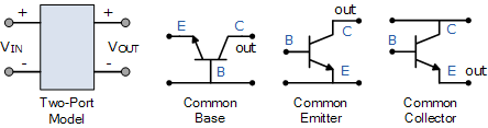
Bipolar Transistor Configurations
As the Bipolar Transistor is a three terminal device, there are basically three possible ways to connect it within an electronic circuit with one terminal being common to both the input and output. Each method of connection responding differently to its input signal within a circuit as the static characteristics of the transistor vary with each circuit arrangement.
· Common Base Configuration – has Voltage Gain but no Current Gain.
· Common Emitter Configuration – has both Current and Voltage Gain.
· Common Collector Configuration – has Current Gain but no Voltage Gain.
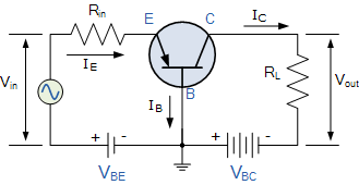
The Common Base (CB) Configuration
As its name suggests, in the Common Base or grounded base configuration, the BASEconnection is common to both the input signal AND the output signal. The input signal is applied between the transistors base and the emitter terminals, while the corresponding output signal is taken from between the base and the collector terminals as shown. The base terminal is grounded or can be connected to some fixed reference voltage point.
The input current flowing into the emitter is quite large as its the sum of both the base current and collector current respectively therefore, the collector current output is less than the emitter current input resulting in a current gain for this type of circuit of “1” (unity) or less, in other words the common base configuration “attenuates” the input signal.
The Common Base Transistor Circuit
his type of amplifier configuration is a non-inverting voltage amplifier circuit, in that the signal voltages Vin and Vout are “in-phase”. This type of transistor arrangement is not very common due to its unusually high voltage gain characteristics. Its input characteristics represent that of a forward biased diode while the output characteristics represent that of an illuminated photo-diode.
Also this type of bipolar transistor configuration has a high ratio of output to input resistance or more importantly “load” resistance ( RL ) to “input” resistance ( Rin ) giving it a value of “Resistance Gain”. Then the voltage gain ( Av ) for a common base configuration is therefore given as:
Common Base Voltage Gain
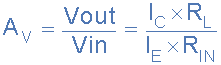
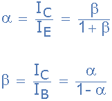
Where: Ic/Ie is the current gain, alpha ( α ) and RL/Rin is the resistance gain.
The common base circuit is generally only used in single stage amplifier circuits such as microphone pre-amplifier or radio frequency ( Rƒ ) amplifiers due to its very good high frequency response.
The Common Emitter (CE) Configuration
In the Common Emitter or grounded emitter configuration, the input signal is applied between the base and the emitter, while the output is taken from between the collector and the emitter as shown. This type of configuration is the most commonly used circuit for transistor based amplifiers and which represents the “normal” method of bipolar transistor connection.
The common emitter amplifier configuration produces the highest current and power gain of all the three bipolar transistor configurations. This is mainly because the input impedance is LOW as it is connected to a forward biased PN-junction, while the output impedance is HIGH as it is taken from a reverse biased PN-junction.
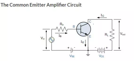
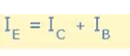
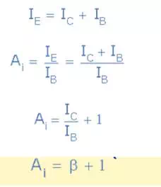
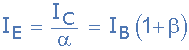
The common emitter configuration has a current gain approximately equal to the β value of the transistor itself. In the common collector configuration the load resistance is situated in series with the emitter so its current is equal to that of the emitter current.
As the emitter current is the combination of the collector AND the base current combined, the load resistance in this type of transistor configuration also has both the collector current and the input current of the base flowing through it. Then the current gain of the circuit is given as:
The Common Collector Current Gain
![]()
Bipolar Transistor Summary
Then to summarise, the behaviour of the bipolar transistor in each one of the above circuit configurations is very different and produces different circuit characteristics with regards to input impedance, output impedance and gain whether this is voltage gain, current gain or power gain and this is summarised in the table below.
Bipolar Transistor Configurations
with the generalised characteristics of the different transistor configurations given in the following table:
|
Characteristic |
Common |
Common |
Common |
|
Input Impedance |
Low |
Medium |
High |
|
Output Impedance |
Very High |
High |
Low |
|
Phase Shift |
0o |
180o |
0o |
|
Voltage Gain |
High |
Medium |
Low |
|
Current Gain |
Low |
Medium |
High |
|
Power Gain |
Low |
Very High |
Medium |
In the next tutorial about Bipolar Transistors, we will look at the NPN Transistor in more detail when used in the common emitter configuration as an amplifier as this is the most widely used configuration due to its flexibility and high gain. We will also plot the output characteristics curves commonly associated with amplifier circuits as a function of the collector current to the base current.