The Zener Diode
A Semiconductor Diode blocks current in the reverse direction, but will suffer from premature breakdown or damage if the reverse voltage applied across becomes too high
However, the Zener Diode or “Breakdown Diode”, as they are sometimes referred too, are basically the same as the standard PN junction diode but they are specially designed to have a low and specified Reverse Breakdown Voltage which takes advantage of any reverse voltage applied to it.
The Zener diode behaves just like a normal general-purpose diode consisting of a silicon PN junction and when biased in the forward direction, that is Anode positive with respect to its Cathode, it behaves just like a normal signal diode passing the rated current.
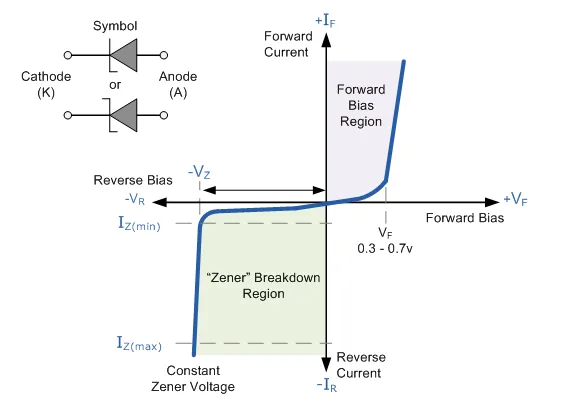
However, unlike a conventional diode that blocks any flow of current through itself when reverse biased, that is the Cathode becomes more positive than the Anode, as soon as the reverse voltage reaches a pre-determined value, the zener diode begins to conduct in the reverse direction.
This is because when the reverse voltage applied across the zener diode exceeds the rated voltage of the device a process called Avalanche Breakdown occurs in the semiconductor depletion layer and a current starts to flow through the diode to limit this increase in voltage.
The current now flowing through the zener diode increases dramatically to the maximum circuit value (which is usually limited by a series resistor) and once achieved, this reverse saturation current remains fairly constant over a wide range of reverse voltages. The voltage point at which the voltage across the zener diode becomes stable is called the “zener voltage”, ( Vz ) and for zener diodes this voltage can range from less than one volt to a few hundred volts.
The point at which the zener voltage triggers the current to flow through the diode can be very accurately controlled (to less than 1% tolerance) in the doping stage of the diodes semiconductor construction giving the diode a specific zener breakdown voltage, ( Vz ) for example, 4.3V or 7.5V. This zener breakdown voltage on the I-V curve is almost a vertical straight line.

The Zener Diode is used in its “reverse bias” or reverse breakdown mode, i.e. the diodes anode connects to the negative supply. From the I-V characteristics curve above, we can see that the zener diode has a region in its reverse bias characteristics of almost a constant negative voltage regardless of the value of the current flowing through the diode and remains nearly constant even with large changes in current as long as the zener diodes current remains between the breakdown current IZ(min) and the maximum current rating IZ(max).
This ability to control itself can be used to great effect to regulate or stabilise a voltage source against supply or load variations. The fact that the voltage across the diode in the breakdown region is almost constant turns out to be an important characteristic of the zener diode as it can be used in the simplest types of voltage regulator applications.
The function of a regulator is to provide a constant output voltage to a load connected in parallel with it in spite of the ripples in the supply voltage or the variation in the load current and the zener diode will continue to regulate the voltage until the diodes current falls below the minimum IZ(min) value in the reverse breakdown region.
Zener Diodes can be used to produce a stabilised voltage output with low ripple under varying load current conditions. By passing a small current through the diode from a voltage source, via a suitable current limiting resistor (RS), the zener diode will conduct sufficient current to maintain a voltage drop of Vout.
We remember from the previous tutorials that the DC output voltage from the half or full-wave rectifiers contains ripple superimposed onto the DC voltage and that as the load value changes so to does the average output voltage. By connecting a simple zener stabiliser circuit as shown below across the output of the rectifier, a more stable output voltage can be produced.
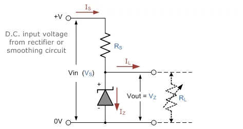
The resistor, RS is connected in series with the zener diode to limit the current flow through the diode with the voltage source, VS being connected across the combination. The stabilised output voltage Vout is taken from across the zener diode. The zener diode is connected with its cathode terminal connected to the positive rail of the DC supply so it is reverse biased and will be operating in its breakdown condition. Resistor RS is selected so to limit the maximum current flowing in the circuit.
With no load connected to the circuit, the load current will be zero, ( IL = 0 ), and all the circuit current passes through the zener diode which in turn dissipates its maximum power. Also a small value of the series resistor RS will result in a greater diode current when the load resistance RL is connected and large as this will increase the power dissipation requirement of the diode so care must be taken when selecting the appropriate value of series resistance so that the zener’s maximum power rating is not exceeded under this no-load or high-impedance condition.
The load is connected in parallel with the zener diode, so the voltage across RL is always the same as the zener voltage, ( VR = VZ ). There is a minimum zener current for which the stabilization of the voltage is effective and the zener current must stay above this value operating under load within its breakdown region at all times. The upper limit of current is of course dependant upon the power rating of the device. The supply voltage VS must be greater than VZ.
One small problem with zener diode stabiliser circuits is that the diode can sometimes generate electrical noise on top of the DC supply as it tries to stabilise the voltage. Normally this is not a problem for most applications but the addition of a large value decoupling capacitor across the zener’s output may be required to give additional smoothing.
Then to summarise a little. A zener diode is always operated in its reverse biased condition. A voltage regulator circuit can be designed using a zener diode to maintain a constant DC output voltage across the load in spite of variations in the input voltage or changes in the load current. The zener voltage regulator consists of a current limiting resistor RS connected in series with the input voltage VS with the zener diode connected in parallel with the load RL in this reverse biased condition. The stabilized output voltage is always selected to be the same as the breakdown voltage VZ of the diode.
A 5.0V stabilised power supply is required to be produced from a 12V DC power supply input source. The maximum power rating PZ of the zener diode is 2W. Using the zener regulator circuit above calculate:
a). The maximum current flowing through the zener diode.

b). The minimum value of the series resistor, RS

c). The load current IL if a load resistor of 1kΩ is connected across the zener diode.

d). The zener current IZ at full load.

As well as producing a single stabilised voltage output, zener diodes can also be connected together in series along with normal silicon signal diodes to produce a variety of different reference voltage output values as shown below.
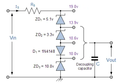
The values of the individual Zener diodes can be chosen to suit the application while the silicon diode will always drop about 0.6 – 0.7V in the forward bias condition. The supply voltage, Vin must of course be higher than the largest output reference voltage and in our example above this is 19v.
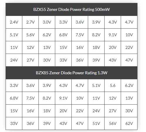
A typical zener diode for general electronic circuits is the 500mW, BZX55 series or the larger 1.3W, BZX85 series were the zener voltage is given as, for example, C7V5 for a 7.5V diode giving a diode reference number of BZX55C7V5.
The 500mW series of zener diodes are available from about 2.4 up to about 100 volts and typically have the same sequence of values as used for the 5% (E24) resistor series with the individual voltage ratings for these small but very useful diodes are given in the table below.
Thus far we have looked at how a zener diode can be used to regulate a constant DC source but what if the input signal was not steady state DC but an alternating AC waveform how would the zener diode react to a constantly changing signal.
Diode clipping and clamping circuits are circuits that are used to shape or modify an input AC waveform (or any sinusoid) producing a differently shape output waveform depending on the circuit arrangement. Diode clipper circuits are also called limiters because they limit or clip-off the positive (or negative) part of an input AC signal. As zener clipper circuits limit or cut-off part of the waveform across them, they are mainly used for circuit protection or in waveform shaping circuits.
For example, if we wanted to clip an output waveform at +7.5V, we would use a 7.5V zener diode. If the output waveform tries to exceed the 7.5V limit, the zener diode will “clip-off” the excess voltage from the input producing a waveform with a flat top still keeping the output constant at +7.5V. Note that in the forward bias condition a zener diode is still a diode and when the AC waveform output goes negative below -0.7V, the zener diode turns “ON” like any normal silicon diode would and clips the output at -0.7V as shown below.
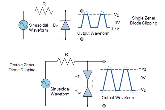
The back to back connected zener diodes can be used as an AC regulator producing what is jokingly called a “poor man’s square wave generator”. Using this arrangement we can clip the waveform between a positive value of +8.2V and a negative value of -8.2V for a 7.5V zener diode.
So for example, if we wanted to clip an output waveform between two different minimum and maximum values of say, +8V and -6V, we would simply use two differently rated zener diodes. Note that the output will actually clip the AC waveform between +8.7V and -6.7V due to the addition of the forward biasing diode voltage.
In other words a peak-to-peak voltage of 15.4 volts instead of expected 14 volts, as the forward bias volt drop across the diode adds another 0.7 volts in each direction.
This type of clipper configuration is fairly common for protecting an electronic circuit from over voltage. The two zener’s are generally placed across the power supply input terminals and during normal operation, one of the zener diodes is “OFF” and the diodes have little or no affect. However, if the input voltage waveform exceeds its limit, then the zener’s turn “ON” and clip the input to protect the circuit.
In the next tutorial about diodes, we will look at using the forward biased PN junction of a diode to produce light. We know from the previous tutorials that when charge carriers move across the junction, electrons combine with holes and energy is lost in the form of heat, but also some of this energy is dissipated as photons but we can not see them.
If we place a translucent lens around the junction, visible light will be produced and the diode becomes a light source. This effect produces another type of diode known commonly as the Light Emitting Diode which takes advantage of this light producing characteristic to emit light (photons) in a variety of colours and wavelengths.