The MOSFET Amplifier
Just like the previous Junction Field Effect transistor, MOSFETs can be used to make single stage class “A” amplifier circuits with the enhancement mode n-channel MOSFET common source amplifier being the most popular circuit. Depletion mode MOSFET amplifiers are very similar to the JFET amplifiers, except that the MOSFET has a much higher input impedance.
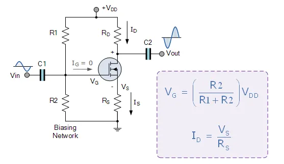
This high input impedance is controlled by the gate biasing resistive network formed by R1 and R2. Also, the output signal for the enhancement mode common source MOSFET amplifier is inverted because when VG is low the transistor is switched “OFF” and VD(Vout) is high. When VG is high the transistor is switched “ON” and VD (Vout) is low as shown.
Enhancement-mode N-Channel MOSFET Amplifier
The DC biasing of this common source (CS) MOSFET amplifier circuit is virtually identical to the JFET amplifier. The MOSFET circuit is biased in class A mode by the voltage divider network formed by resistors R1 and R2. The AC input resistance is given as RIN = RG = 1MΩ.
Metal Oxide Semiconductor Field Effect Transistors are three terminal active devices made from different semiconductor materials that can act as either an insulator or a conductor by the application of a small signal voltage.
The MOSFETs ability to change between these two states enables it to have two basic functions: “switching” (digital electronics) or “amplification” (analogue electronics). Then MOSFETs have the ability to operate within three different regions:
· 1. Cut-off Region – with VGS < Vthreshold the gate-source voltage is much lower than the transistors threshold voltage so the MOSFET transistor is switched “fully-OFF” thus, ID = 0, with the transistor acting like an open switch regardless of the value of VDS.
· 2. Linear (Ohmic) Region – with VGS > Vthreshold and VDS < VGS the transistor is in its constant resistance region behaving as a voltage-controlled resistance whose resistive value is determined by the gate voltage, VGS level.
· 3. Saturation Region – with VGS > Vthreshold and VDS > VGS the transistor is in its constant current region and is therefore “fully-ON”. The Drain current ID = Maximum with the transistor acting as a closed switch.