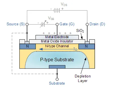
Basic MOSFET Structure and Symbol
The construction of the Metal Oxide Semiconductor FET is very different to that of the Junction FET. Both the Depletion and Enhancement type MOSFETs use an electrical field produced by a gate voltage to alter the flow of charge carriers, electrons for n-channel or holes for P-channel, through the semiconductive drain-source channel. The gate electrode is placed on top of a very thin insulating layer and there are a pair of small n-type regions just under the drain and source electrodes.
We saw in the previous tutorial, that the gate of a junction field effect transistor, JFET must be biased in such a way as to reverse-bias the pn-junction. With a insulated gate MOSFET device no such limitations apply so it is possible to bias the gate of a MOSFET in either polarity, positive (+ve) or negative (-ve).
This makes the MOSFET device especially valuable as electronic switches or to make logic gates because with no bias they are normally non-conducting and this high gate input resistance means that very little or no control current is needed as MOSFETs are voltage controlled devices. Both the p-channel and the n-channel MOSFETs are available in two basic forms, the Enhancement type and the Depletion type.