The MOSFET
MOSFET’s operate the same as JFET’s but have a gate terminal that is electrically isolated from the conductive channel.
As well as the Junction Field Effect Transistor (JFET), there is another type of Field Effect Transistor available whose Gate input is electrically insulated from the main current carrying channel and is therefore called an Insulated Gate Field Effect Transistor.
The most common type of insulated gate FET which is used in many different types of electronic circuits is called the Metal Oxide Semiconductor Field Effect Transistor or MOSFET for short.
The IGFET or MOSFET is a voltage controlled field effect transistor that differs from a JFET in that it has a “Metal Oxide” Gate electrode which is electrically insulated from the main semiconductor n-channel or p-channel by a very thin layer of insulating material usually silicon dioxide, commonly known as glass.
This ultra thin insulated metal gate electrode can be thought of as one plate of a capacitor. The isolation of the controlling Gate makes the input resistance of the MOSFETextremely high way up in the Mega-ohms ( MΩ ) region thereby making it almost infinite.
As the Gate terminal is electrically isolated from the main current carrying channel between the drain and source, “NO current flows into the gate” and just like the JFET, the MOSFET also acts like a voltage controlled resistor where the current flowing through the main channel between the Drain and Source is proportional to the input voltage. Also like the JFET, the MOSFETs very high input resistance can easily accumulate large amounts of static charge resulting in the MOSFET becoming easily damaged unless carefully handled or protected.
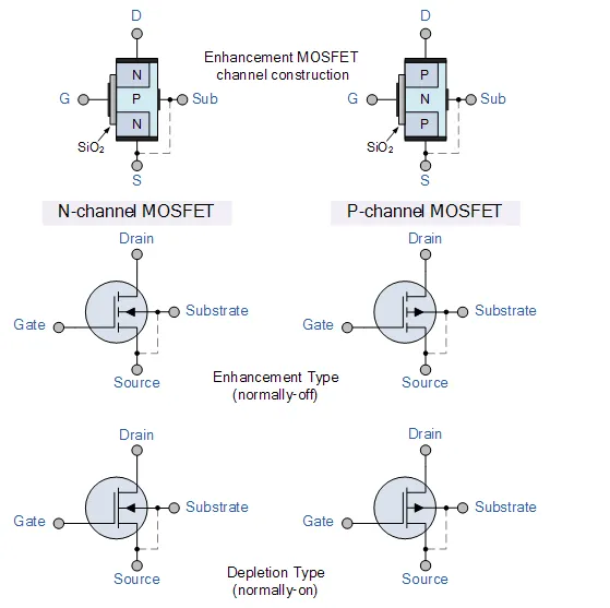
Like the previous JFET tutorial, MOSFETs are three terminal devices with a Gate, Drainand Source and both P-channel (PMOS) and N-channel (NMOS) MOSFETs are available. The main difference this time is that MOSFETs are available in two basic forms:
· Depletion Type – the transistor requires the Gate-Source voltage, ( VGS ) to switch the device “OFF”. The depletion mode MOSFET is equivalent to a “Normally Closed” switch.
· Enhancement Type – the transistor requires a Gate-Source voltage, ( VGS ) to switch the device “ON”. The enhancement mode MOSFET is equivalent to a “Normally Open” switch.
The symbols and basic construction for both configurations of MOSFETs are shown below.
The four MOSFET symbols above show an additional terminal called the Substrate and is not normally used as either an input or an output connection but instead it is used for grounding the substrate. It connects to the main semiconductive channel through a diode junction to the body or metal tab of the MOSFET.
Usually in discrete type MOSFETs, this substrate lead is connected internally to the source terminal. When this is the case, as in enhancement types it is omitted from the symbol for clarification.
The line in the MOSFET symbol between the drain (D) and source (S) connections represents the transistors semiconductive channel. If this channel line is a solid unbroken line then it represents a “Depletion” (normally-ON) type MOSFET as drain current can flow with zero gate biasing potential.
If the channel line is shown as a dotted or broken line, then it represents an “Enhancement” (normally-OFF) type MOSFET as zero drain current flows with zero gate potential. The direction of the arrow pointing to this channel line indicates whether the conductive channel is a P-type or an N-type semiconductor device.