The JFET Amplifier
Just like the bipolar junction transistor, JFET’s can be used to make single stage class A amplifier circuits with the JFET common source amplifier and characteristics being very similar to the BJT common emitter circuit. The main advantage JFET amplifiers have over BJT amplifiers is their high input impedance which is controlled by the Gate biasing resistive network formed by R1 and R2 as shown.
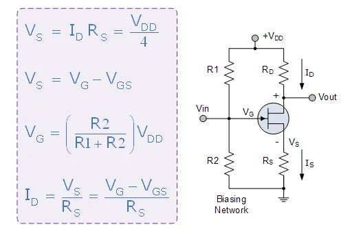
Biasing of JFET Amplifier
This common source (CS) amplifier circuit is biased in class “A” mode by the voltage divider network formed by resistors R1 and R2. The voltage across the Source resistor RS is generally set to be about one quarter of VDD, ( VDD /4 ) but can be any reasonable value.
The required Gate voltage can then be calculated from this RS value. Since the Gate current is zero, (IG = 0) we can set the required DC quiescent voltage by the proper selection of resistors R1 and R2.
The control of the Drain current by a negative Gate potential makes the Junction Field Effect Transistor useful as a switch and it is essential that the Gate voltage is never positive for an N-channel JFET as the channel current will flow to the Gate and not the Drain resulting in damage to the JFET. The principals of operation for a P-channel JFET are the same as for the N-channel JFET, except that the polarity of the voltages need to be reversed.