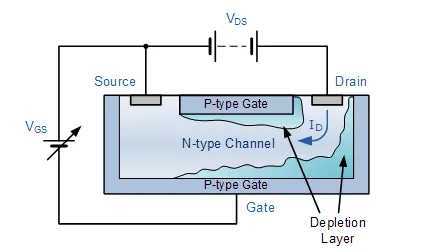
Biasing of an N-channel JFET

The cross sectional diagram above shows an N-type semiconductor channel with a P-type region called the Gate diffused into the N-type channel forming a reverse biased PN-junction and it is this junction which forms the depletion region around the Gate area when no external voltages are applied. JFETs are therefore known as depletion mode devices.
This depletion region produces a potential gradient which is of varying thickness around the PN-junction and restrict the current flow through the channel by reducing its effective width and thus increasing the overall resistance of the channel itself.
Then we can see that the most-depleted portion of the depletion region is in between the Gate and the Drain, while the least-depleted area is between the Gate and the Source. Then the JFET’s channel conducts with zero bias voltage applied (ie, the depletion region has near zero width).
With no external Gate voltage ( VG = 0 ), and a small voltage ( VDS ) applied between the Drain and the Source, maximum saturation current ( IDSS ) will flow through the channel from the Drain to the Source restricted only by the small depletion region around the junctions.
If a small negative voltage ( -VGS ) is now applied to the Gate the size of the depletion region begins to increase reducing the overall effective area of the channel and thus reducing the current flowing through it, a sort of “squeezing” effect takes place. So by applying a reverse bias voltage increases the width of the depletion region which in turn reduces the conduction of the channel.
Since the PN-junction is reverse biased, little current will flow into the gate connection. As the Gate voltage ( -VGS ) is made more negative, the width of the channel decreases until no more current flows between the Drain and the Source and the FET is said to be “pinched-off” (similar to the cut-off region for a BJT). The voltage at which the channel closes is called the “pinch-off voltage”, ( VP ).
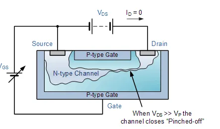
In this pinch-off region the Gate voltage, VGS controls the channel current and VDS has little or no effect.
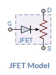
The result is that the FET acts more like a voltage controlled resistor which has zero resistance when VGS = 0 and maximum “ON” resistance ( RDS ) when the Gate voltage is very negative. Under normal operating conditions, the JFET gate is always negatively biased relative to the source.
It is essential that the Gate voltage is never positive since if it is all the channel current will flow to the Gate and not to the Source, the result is damage to the JFET. Then to close the channel:
· No Gate Voltage ( VGS ) and VDS is increased from zero.
· No VDS and Gate control is decreased negatively from zero.
· VDS and VGS varying.
The P-channel Junction Field Effect Transistor operates exactly the same as the N-channel above, with the following exceptions: 1). Channel current is positive due to holes, 2). The polarity of the biasing voltage needs to be reversed.
The output characteristics of an N-channel JFET with the gate short-circuited to the source is given as:
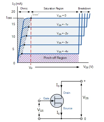
The voltage VGS applied to the Gate controls the current flowing between the Drain and the Source terminals. VGS refers to the voltage applied between the Gate and the Source while VDS refers to the voltage applied between the Drain and the Source.
Because a Junction Field Effect Transistor is a voltage controlled device, “NO current flows into the gate!” then the Source current ( IS ) flowing out of the device equals the Drain current flowing into it and therefore ( ID = IS ).
The characteristics curves example shown above, shows the four different regions of operation for a JFET and these are given as:
· Ohmic Region – When VGS = 0 the depletion layer of the channel is very small and the JFET acts like a voltage controlled resistor.
· Cut-off Region – This is also known as the pinch-off region were the Gate voltage, VGS is sufficient to cause the JFET to act as an open circuit as the channel resistance is at maximum.
· Saturation or Active Region – The JFET becomes a good conductor and is controlled by the Gate-Source voltage, ( VGS ) while the Drain-Source voltage, ( VDS) has little or no effect.
· Breakdown Region – The voltage between the Drain and the Source, ( VDS ) is high enough to causes the JFET’s resistive channel to break down and pass uncontrolled maximum current.
The characteristics curves for a P-channel junction field effect transistor are the same as those above, except that the Drain current ID decreases with an increasing positive Gate-Source voltage, VGS.
The Drain current is zero when VGS = VP. For normal operation, VGS is biased to be somewhere between VP and 0. Then we can calculate the Drain current, ID for any given bias point in the saturation or active region as follows:

Note that the value of the Drain current will be between zero (pinch-off) and IDSS(maximum current). By knowing the Drain current ID and the Drain-Source voltage VDSthe resistance of the channel ( RDS ) is given as:

Where: gm is the “transconductance gain” since the JFET is a voltage controlled device and which represents the rate of change of the Drain current with respect to the change in Gate-Source voltage.
Like the bipolar junction transistor, the field effect transistor being a three terminal device is capable of three distinct modes of operation and can therefore be connected within a circuit in one of the following configurations.