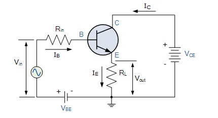
The Common Collector (CC) Configuration
In the Common Collector or grounded collector configuration, the collector is now common through the supply. The input signal is connected directly to the base, while the output is taken from the emitter load as shown. This type of configuration is commonly known as a Voltage Follower or Emitter Follower circuit.
The common collector, or emitter follower configuration is very useful for impedance matching applications because of the very high input impedance, in the region of hundreds of thousands of Ohms while having a relatively low output impedance.
The Common Collector Transistor Circuit
The common emitter configuration has a current gain approximately equal to the β value of the transistor itself. In the common collector configuration the load resistance is situated in series with the emitter so its current is equal to that of the emitter current.
As the emitter current is the combination of the collector AND the base current combined, the load resistance in this type of transistor configuration also has both the collector current and the input current of the base flowing through it. Then the current gain of the circuit is given as:
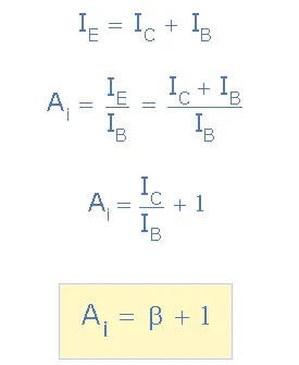
This type of bipolar transistor configuration is a non-inverting circuit in that the signal voltages of Vin and Vout are “in-phase”. It has a voltage gain that is always less than “1” (unity). The load resistance of the common collector transistor receives both the base and collector currents giving a large current gain (as with the common emitter configuration) therefore, providing good current amplification with very little voltage gain.
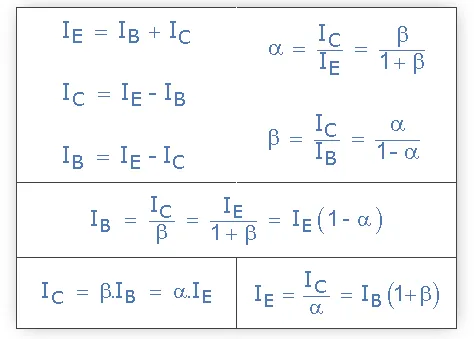
We can now summarise the various relationships between the transistors individual DC currents flowing through each leg and its DC current gains given above in the following table.