SEMICONDUCTOR MATERIALS
The label semiconductor itself provides a hint as to its characteristics. The prefix semi – is normally applied to a range of levels midway between two limits.
The term conductor is applied to any material that will support a generous flow of charge when a voltage source of limited magnitude is applied across its terminals. An insulator is a material that offers a very low level of conductivity under pressure from an applied voltage source. A semiconductor, therefore, is a material that has a conductivity level somewhere between the extremes of an insulator and a conductor.
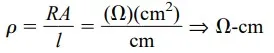
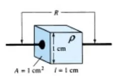
Inversely related to the conductivity of a material is its resistance to the flow of charge, or current. That is, the higher the conductivity level, the lower the resistance level. In tables, the term resistivity (ρ, Greek letter rho) is often used when comparing the resistance levels of materials. In metric units, the resistivity of a material is measured in Ω-cm or Ω-m. The units of Ω-cm are derived from the substitution of the units for each quantity of Fig. 1.4 into the following equation (derived from the basic resistance equation R = ρl/A):
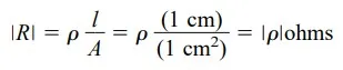
In fact, if the area of Fig. is 1 cm2 and the length 1 cm, the magnitude of the resistance of the cube of Fig. is equal to the magnitude of the resistivity of the material as demonstrated below:
This fact will be helpful to remember as we compare resistivity levels in the discussions to follow
In Table, typical resistivity values are provided for three broad categories of materials. Although you may be familiar with the electrical properties of copper and mica from your past studies, the characteristics of the semiconductor materials of germanium (Ge) and silicon (Si) may be relatively new. As you will find in the chapters to follow, they are certainly not the only two semiconductor materials. They are, however, the two materials that have received the broadest range of interest in the development of semiconductor devices. In recent years the shift has been steadily toward silicon and away from germanium, but germanium is still in modest production.
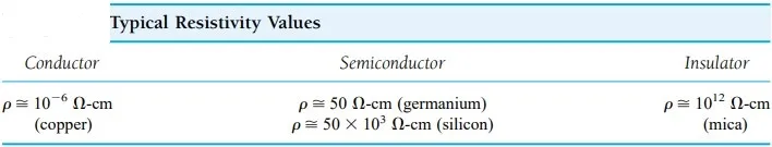
Note in Table the extreme range between the conductor and insulating materials for the 1-cm length (1-cm2 area) of the material. Eighteen places separate the placement of the decimal point for one number from the other. Ge and Si have received the attention they have for a number of reasons. One very important consideration is the fact that they can be manufactured to a very high purity level. In fact, recent advances have reduced impurity levels in the pure material to 1 part in 10 billion (110,000,000,000). One might ask if these low impurity levels are really necessary. They certainly are if you consider that the addition of one part impurity (of the proper type) per million in a wafer of silicon material can change that material from a relatively poor conductor to a good conductor of electricity. We are obviously dealing with a whole new spectrum of comparison levels when we deal with the semiconductor medium. The ability to change the characteristics of the material significantly through this process, known as “doping,” is yet another reason why Ge and Si have received such wide attention. Further reasons include the fact that their characteristics can be altered significantly through the application of heat or light—an important consideration in the development of heat- and light-sensitive devices.
Intrinsic materials are those semiconductors that have been carefully refined to reduce the impurities to a very low level—essentially as pure as can be made available through modern technology.
The free electrons in the material due only to natural causes are referred to as intrinsic carriers. At the same temperature, intrinsic germanium material will have approximately 2.5 x 10¹³ free carriers per cubic centimeter. The ratio of the number of carriers in germanium to that of silicon is greater than 103 and would indicate that germanium is a better conductor at room temperature. This may be true, but both are still considered poor conductors in the intrinsic state. Note in Table above that the resistivity also differs by a ratio of about 1000 : 1, with silicon having the larger value. This should be the case, of course, since resistivity and conductivity are inversely related.
An increase in temperature of a semiconductor can result in a substantial increase in the number of free electrons in the material.
As the temperature rises from absolute zero (0 K), an increasing number of valence electrons absorb sufficient thermal energy to break the covalent bond and contribute to the number of free carriers as described above. This increased number of carriers will increase the conductivity index and result in a lower resistance level.
Semiconductor materials such as Ge and Si that show a reduction in resistance with increase in temperature are said to have a negative temperature coefficient.
You will probably recall that the resistance of most conductors will increase with temperature. This is due to the fact that the numbers of carriers in a conductor will not increase significantly with temperature, but their vibration pattern about a relatively fixed location will make it increasingly difficult for electrons to pass through. An increase in temperature therefore results in an increased resistance level and a positive temperature coefficient.