The Clipper circuit that is intended to attenuate positive portions of the input signal can be termed as a Positive Clipper. Among the positive diode clipper circuits, we have the following types −
Let us discuss each of these types in detail.
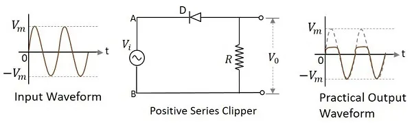
A Clipper circuit in which the diode is connected in series to the input signal and that attenuates the positive portions of the waveform, is termed as Positive Series Clipper. The following figure represents the circuit diagram for positive series clipper.
Positive Cycle of the Input − When the input voltage is applied, the positive cycle of the input makes the point A in the circuit positive with respect to the point B. This makes the diode reverse biased and hence it behaves like an open switch. Thus the voltage across the load resistor becomes zero as no current flows through it and hence V0V0 will be zero.
Negative Cycle of the Input − The negative cycle of the input makes the point A in the circuit negative with respect to the point B. This makes the diode forward biased and hence it conducts like a closed switch. Thus the voltage across the load resistor will be equal to the applied input voltage as it completely appears at the output V0V0.
In the above figures, if the waveforms are observed, we can understand that only a portion of the positive peak was clipped. This is because of the voltage across V0. But the ideal output was not meant to be so. Let us have a look at the following figures.
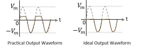
Unlike the ideal output, a bit portion of the positive cycle is present in the practical output due to the diode conduction voltage which is 0.7v. Hence there will be a difference in the practical and ideal output waveforms.
A Clipper circuit in which the diode is connected in series to the input signal and biased with positive reference voltage VrVr and that attenuates the positive portions of the waveform, is termed as Positive Series Clipper with positive VrVr. The following figure represents the circuit diagram for positive series clipper when the reference voltage applied is positive.
During the positive cycle of the input the diode gets reverse biased and the reference voltage appears at the output. During its negative cycle, the diode gets forward biased and conducts like a closed switch. Hence the output waveform appears as shown in the above figure.
A Clipper circuit in which the diode is connected in series to the input signal and biased with negative reference voltage VrVr and that attenuates the positive portions of the waveform, is termed as Positive Series Clipper with negative VrVr. The following figure represents the circuit diagram for positive series clipper, when the reference voltage applied is negative.
During the positive cycle of the input the diode gets reverse biased and the reference voltage appears at the output. As the reference voltage is negative, the same voltage with constant amplitude is shown. During its negative cycle, the diode gets forward biased and conducts like a closed switch. Hence the input signal that is greater than the reference voltage, appears at the output.
A Clipper circuit in which the diode is connected in shunt to the input signal and that attenuates the positive portions of the waveform, is termed as Positive Shunt Clipper. The following figure represents the circuit diagram for positive shunt clipper.
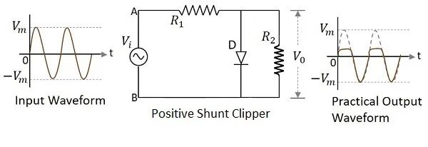
Positive Cycle of the Input − When the input voltage is applied, the positive cycle of the input makes the point A in the circuit positive with respect to the point B. This makes the diode forward biased and hence it conducts like a closed switch. Thus the voltage across the load resistor becomes zero as no current flows through it and hence V0V0 will be zero.
Negative Cycle of the Input − The negative cycle of the input makes the point A in the circuit negative with respect to the point B. This makes the diode reverse biased and hence it behaves like an open switch. Thus the voltage across the load resistor will be equal to the applied input voltage as it completely appears at the output V0V0.
In the above figures, if the waveforms are observed, we can understand that only a portion of the positive peak was clipped. This is because of the voltage across V0V0. But the ideal output was not meant to be so. Let us have a look at the following figures.
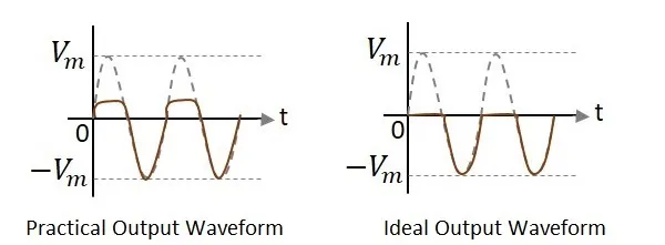
Unlike the ideal output, a bit portion of the positive cycle is present in the practical output due to the diode conduction voltage which is 0.7v. Hence there will be a difference in the practical and ideal output waveforms.
A Clipper circuit in which the diode is connected in shunt to the input signal and biased with positive reference voltage VrVr and that attenuates the positive portions of the waveform, is termed as Positive Shunt Clipper with positive VrVr. The following figure represents the circuit diagram for positive shunt clipper when the reference voltage applied is positive.
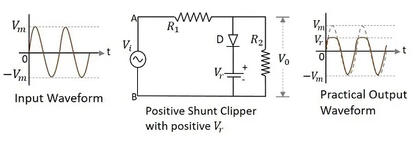
During the positive cycle of the input the diode gets forward biased and nothing but the reference voltage appears at the output. During its negative cycle, the diode gets reverse biased and behaves as an open switch. The whole of the input appears at the output. Hence the output waveform appears as shown in the above figure.
A Clipper circuit in which the diode is connected in shunt to the input signal and biased with negative reference voltage VrVr and that attenuates the positive portions of the waveform, is termed as Positive Shunt Clipper with negative VrVr.
The following figure represents the circuit diagram for positive shunt clipper, when the reference voltage applied is negative.
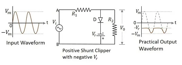
During the positive cycle of the input, the diode gets forward biased and the reference voltage appears at the output. As the reference voltage is negative, the same voltage with constant amplitude is shown. During its negative cycle, the diode gets reverse biased and behaves as an open switch. Hence the input signal that is greater than the reference voltage, appears at the output.