Single Crystal Growth
|
Ø We now have hyperpure poly-Si, already doped to the desired level, and the next step must be to convert it to a single crystal. There are essentially two methods for crystal growth used in this case: |
|||
|
· Float zone or FZ crystals. |
|||
|
Ø The latter method produces crystals with the highest purity, but is not easily used at large diameters. 150 mm crystals are already quite difficult to make and nobody so far has made a 300 mm crystal this way. Float zone crystal growth, while the main method at the beginning of the Si age, is now only used for some specialities and therefore will not be discussed here; some details can be found in the link. |
|||
|
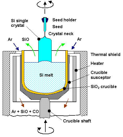
· The Czochralski method, invented by the Polish scientist J. Czochralski in 1916, is the method of choice for high volume production of Si single crystals of exceptional quality and shall be discussed briefly. Below is a schematic drawing of a crystal growth apparatus employing the Czochralski method. More details can be found in the link. |
|||
|
|||
|
· Essentially, a crystal is "pulled" out of a vessel containing liquid Si by dipping a seed crystal into the liquid which is subsequently slowly withdrawn at a surface temperature of the melt just above the melting point. |
|||
|
· The pulling rate (usually a few mm/min) and the temperature profile determines the crystal diameter (the problem is to get rid of the heat of crystallization). |
|||
|
· Everything else determines the quality and homogeneity - crystal growing is still as much an art as a science! Some interesting points are contained in the link. |
|||
|
Ø Here we only look at one major point, the segregation coefficient kseg of impurity atoms. |
|||
|
· The segregation coefficient in thermodynamic equilibrium gives the relation between the concentration of impurity atoms in the growing crystal and that of the melt. It is usually much lower than 1 because impurity atoms "prefer" to stay in the melt. This can be seen from the liquidus and solidus lines in the respective phase diagrams. |
|||
|
· In other words, the solubility of impurity atoms in the melt is larger than in the solid. |
|||
|
· "Equilibrium" refers to a growth speed of 0 mm/min or, more practically, very low growth rates. For finite growth rates, kseg becomes a function of the growth rate (called kseff) and approximates 1 for high growth rates (whatever comes to the rapidly moving interface gets incorporated). |
|||
|
Ø This has a positive and a negative side to it: |
|||||||||||||||||||||||||||||||||||||
|
· On the positive side, the crystal will be cleaner than the liquid, crystal growing is simultaneously a purification method. Always provided that we discard the last part of the crystal where all the impurities are now concentrated. After all, what was in the melt must be in the solid after solidification - only the distribution may now be different. |
|||||||||||||||||||||||||||||||||||||
|
· This defines the negative side: The distribution of impurities - and that includes the doping elements and oxygen - will change along the length of a crystal - a homogeneous doping etc. is difficult to achieve. |
|||||||||||||||||||||||||||||||||||||
|
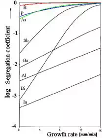
· That segregation can be a large effect with a sensitive dependence on the growth rate is shown below for the possible doping elements; the segregation coefficients of the unwanted impurities is given in a table. |
|||||||||||||||||||||||||||||||||||||
|
|
|
|||||||||||||||||||||||||||||||||||
|
· We recognize one reason why practically only As, P, and B is used for doping! Their segregation coefficient is close to 1 which assures half-way homogeneous distribution during crystal growth. Achieving homogeneous doping with Bi, on the other hand, would be exceedingly difficult or just impossible. |
|||||||||||||||||||||||||||||||||||||
|
Ø Present day single crystals of silicon are the most perfect objects on this side of Pluto - remember that perfection can be measured by using the second law of thermodynamics; this is not an empty statement! A very interesting and readable article dealing with the history and the development of Si crystal growth from W. Zulehner (Wacker Siltronic), who was working on this subject from the very beginning of commercial Si crystal growth until today, can be found in the link. |
|||||||||||||||||||||||||||||||||||||
|
· What the finished crystal looks like can be seen in the link. What we cannot see is that there is no other crystal of a different material that even comes close in size and perfection. |
|||||||||||||||||||||||||||||||||||||
|
· Our crystal does not contain dislocations - a unique feature that only could be matched by Germanium crystals at appreciable sizes (which nobody grows or needs)1). It also does not contain many other lattice defects. With the exception of the doping atoms (and possible interstitial oxygen, which often is wanted in a concentration of about 30 ppm), substitutional and interstitial impurities are well below a ppb if not ppt level (except for relatively harmless carbon at about 1 ppm) - unmatched by most other "high purity" materials. |
|||||||||||||||||||||||||||||||||||||
|
· Our crystal is homogeneous. The concentration of the doping atoms (and possibly interstitial oxygen) is radially and laterally rather constant, a feat not easily achieved. |
|||||||||||||||||||||||||||||||||||||
|
Ø The crystal is now ready for cutting into wafers. |
|||||||||||||||||||||||||||||||||||||
|
|
|||||||||||||||||||||||||||||||||||||
|
Wafer Technology |
||||
|
|
||||
|
· It may appear rather trivial now to cut the crystal into slices which, after some polishing, result in the wafers used as the starting material for chip production. |
||||
|
· However, it is not trivial. While a wafer does not look like much, its not easy to manufacture. Again, making wafers is a closely guarded secret and it is possibly even more difficult to see a wafer production than a single Sicrystal production. |
||||
|
· First, wafers must all be made to exceedingly tight geometric specifications. Not only must the diameter and the thickness be precisely what they ought to be, but the flatness is constrained to about 1 µm. |
||||
|
· This means that the polished surface deviates at most about 1 µm from an ideally flat reference plane - for surface areas of more than 1000 cm2 for a 300 mm wafer! |
||||
|
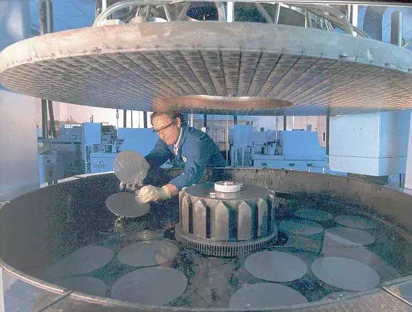
· And this is not just true for one wafer, but for all 10.000 or so produced daily in one factory. The number of Si wafers sold in 2001 is about 100.000.000 or roughly 300.000 a day! Only tightly controlled processes with plenty of know-how and expensive equipment will assure these specifications. The following picture gives an impression of the first step of a many-step polishing procedure. |
||||
|
||||
|
|
In contrast to e.g. polished metals, polished Si wafers have a perfect surface - the crystal just ends followed by less than two nm of "native oxide" which forms rather quickly in air and protects the wafer from chemical attacks. |
||||
|
|
Polishing Si is not easy (but fairly well understood) and so is keeping the surface clean of particles. The final polishing and cleaning steps are done in a cleanroom where the wafers are packed for shipping. |
||||
|
|
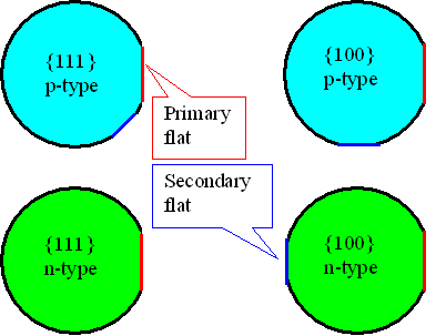
Since chip structures are always aligned along crystallographic directions, it is important to indicate the crystallography of a wafer. This is done by grinding flats (or, for very large wafer - 200 mm and beyond notches) at precisely defined positions. |
||||
|
|
The flats also encode the doping types - mix ups are very expensive! The convention for flats is as follows: |
||||
|
|
|||||
|
|
The main flat is always along a <110> direction. However, many companies have special agreements with wafer producers and have "customized" flats (most commonly no secondary flat on {100} p-type material). |
|||
|
|
|
|
More about flats in the link |
||
|
|
|||||
|
· Typical wafer specifications may contain more than 30 topics, the most important ones are: |
|||||
|
|
· Doping type: n or p-type (p-type is by far the most common type) and dopant used (P, As or B). Resistivity (commonly between 100 Ωcm to 0,001 Ωcm with (5 - 1) Ωcm defining the bulk of the business. All numbers with error margins and homogeneity requirements |
||||
|
|
· Impurity concentrations for metals and other "life time killers" (typically below 1012 cm–3), together with the life time or diffusion length (which should be several 100 µm). |
||||
|
|
· Oxygen and carbon concentration (typically around 6 · 1017 cm–3 or 1 · 1016 cm–3, respectively. While the carbon concentration just has to be low, the oxygen concentration often is specified within narrow limits because the customer may use "internal gettering", a process where oxygen precipitates are formed intensionally in the bulk of the wafer with beneficial effects on the chips in the surface near regions. |
||||
|
|
· Microdefect densities (after all, the point defects generated in thermal equilibrium during crystal growth must still be there in the form of small agglomerates). The specification here may simple be: BMD ("bulk micro defect") density = 0 cm–3. Which simply translates into: Below the detection limit of the best analytical tools. |
||||
|
|
· Geometry, especially several parameters relating to flatness. Typical tolerances are always in the 1 µm regime. |
||||
|
|
· Surface cleanliness: No particles and no atomic or molecular impurities on the surface! |
||||
|
· This link provides a grapical overview of the complete production process - from sand to Si wafers - and includes a few steps not covered here. |
|||||
|
· Appreciate that the production of wafers - at last several thousands per day - with specifications that are always at the cutting edge of what is possible - is an extremely involved and difficult process. |
|||||
|
· At present (Jan. 2004), there are only a handfull of companies world wide that can do it. In fact, 4 companies control about 80% of the market. |
|||||
|
· This link leads to a recent (1999) article covering new developments in Si CZ crystal growth and wafer technology (from A.P. Mozer; Wacker Siltronic) and gives an impression of the richness of complex issues behind the production of the humble Si wafer. |
|||||
|
· This link shows commercial wafer specifications. |
|||||
|
· To give an idea of the size iof the industry: In 2004 a grand totoal of about 4.000.000 m2 of polished Si wafers was produced, equivalent to about 1.25 · 108 200 mm wafers. |
|||||