Monolithic IC – Component Fabrication
Now we shall discuss in detail how different circuit elements like capacitors, transistors, diodes, and resistors are fabricated into an IC. Please note that it is practically impossible to fabricate an inductor into an IC. It is thus added externally by connecting it to the corresponding IC pin as designed by the manufacturer.
Transistors
The fabrication process of a transistor is shown in the figure below. A P-type substrate is first grown and then the collector, emitter, and base regions are diffused on top of it as shown in the figure. The surface terminals for these regions are also provided for connection.
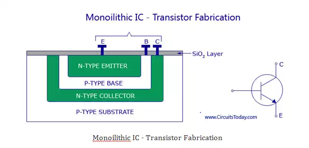
Both transistors and diodes are fabricated by using the epitaxial planar diffusion process that is explained earlier. In case of discrete transistors, the P-type substrate is considered as the collector. `But this is not possible in monolithic IC’s, as all the transistors connected on one P-type substrate would have their collectors connected together. This is why separate collector regions are diffused into the substrate. Even though separate collector regions are formed, they are not completely isolated from the substrate. For proper functioning of the circuit it is necessary that the P-type substrate is always kept negative with respect to the transistor collector. This is achieved by connecting the substrate to the most negative terminal of the circuit supply. The unwanted or parasitic junctions, even when reverse-biased, can still affect the circuit performance adversely. The junction reverse leakage current can cause a serious problem in circuits operating at very low current levels. The capacitance of the reverse-biased junction may affect the circuit high-frequency performance, and the junction break down voltage imposes limits on the usable level of supply voltage. All these adverse effects can be reduced to the minimum if highly resistive material is employed for the substrate. If the substrate is very lightly doped, it will behave almost as an insulator.
Diodes
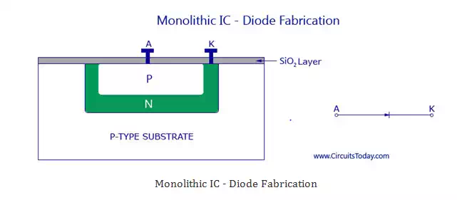
They are also fabricated by the same diffusion process as transistors are. The only difference is that only two of the regions are used to form one P-N junction. In figure, collector-base junction of the transistor is used as a diode. Anode of the diode is formed during the base diffusion of the transistor and the collector region of the transistor becomes the cathode of the diode. For high speed switching emitter base junction is used as a diode.
Resistors
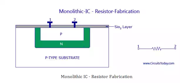
The resistors used in IC’s are given their respective ohmic value by varying the concentration of doping impurity and depth of diffusion. The range of resistor values that may be produced by the diffusion process varies from ohms to hundreds of kilohms. The typical tolerance, however, may be no better than ± 5%, and may even be as high as ± 20%. On the other hand, if all the resistors are diffused at the same time, then the tolerance ratio may be good. Most resistors are formed during the base diffusion of the integrated transistor, as shown in figure below. This is because it is the highest resistivity region. For low resistance values, emitter region is used as it has much lower resistivity.
Another diffusion technique is also used for the growth of IC resistors. It is basically a thin-film technique. In this process a metal film is deposited on a glass or Si02 surface. The resistance value can be controlled by varying thickness, width and length of the film. Since diffused resistors can be processed while diffusing transistors. This technique is more economic and less time consuming and therefore, the most widely used.
Capacitors
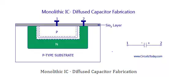
The figure below shows the P and N-regions forming the capacitor plates. The dielectric of the capacitor is the depletion region between them.
All P-N junctions have capacitance so capacitors may be produced by fabricating junctions. The amount of change in the reverse bias varies the value of junction capacitance and also the depletion width. The value may be as less as 100 picoFarads.
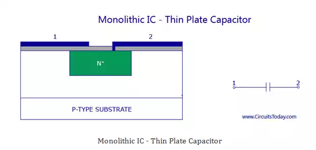
Using the silicon dioxide as a dielectric may also be a way to fabricate capacitors. One plate of the capacitors is formed by diffusing a heavily doped N-region. The other plate of the capacitor is formed by depositing a film of aluminium on the silicon dioxide dielectric on the wafer surface. For such a capacitor, a voltage of any polarity can be used, and when comparing a diffused capacitor with such a capacitor the diffused capacitor may have very small values of breakdown voltage.