Monolithic IC Manufacturing Process
For the manufacture and production of the monolithic IC, all circuit components and their interconnections are to be formed in a single thin wafer. The different processes carried out for achieving this are explained below.
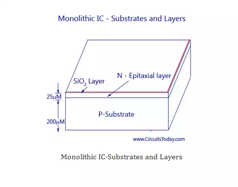
P-layer Substrate Manufacture
Being the base layer of the IC, the P-type is silicon is first built for the IC. A silicon crystal of P-type is grown in dimensions of 250mm length and 25mm diameter. The silicon is then cut into thin slices with high precision using a diamond saw. Each wafer will precisely have a thickness of 200 micrometer and a diameter of 25 mm. These thin slices are termed wafers. These wafers may be circular or rectangular in shape with respect to the shape of the IC. After cutting hundreds of them each wafer is polished and cleaned to form a P-type substrate layer.
N-type Epitaxial Growth
The epitaxial groth process of a low resistive N-type over a high resistive P-type is to be carried out. This is done by placing the n-type layer on top of the P-type and heating then inside a diffusion furnace at very high temperature (nearly 1200C). After heating, a gas mixture f Silicon atoms and pentavalent atoms are also passed over the layer. This forms the epitaxial layer on the substrate. All the components required for the circuit are built on top of this layer. The layer is then cooled down, polished and cleaned.
The Silicon Dioxide Insulation Layer
As explained above, this layer is required contamination of the N-layer epitaxy. This layer is only 1 micrometer thin and is grown by exposing the epitaxial layer to oxygen atmosphere at 1000C. A detailed image showing the P-type, N-type epitaxial layer and SiO2 layer is given below.
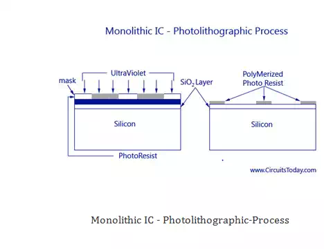
Photolithographic Process for SiO2
To diffuse the impurities with the N-type epitaxial region, the silicon dioxide layer has to be etched in selected areas. Thus openings must be brought at these areas through photolithographic process. In this process, the SiO2 layer is coated with a thin layer of a photosensitive material called photoresist. A large black and white pattern is made in the desired patter, where the black pattern represents the area of opening and white represents the area that is left idle. This pattern is reduced in size and fit to the layer, above the photoresist. The whole layer is then exposed to ultraviolet light. Due to the exposure, the photoresist right below the white pattern becomes polymerized. The pattern is then removed and the wafer is developed using a chemical like trichloroethylene. The chemical dissolves the unpolymerized portion of the photoresist film and leaves the surface. The oxide not covered by polymerised photoresist is then removed by immersing the chip in an etching solution of HCl. Those portions of the Si02 which are protected by the photoresist remain unaffected by the acid. After the etching and diffusion process, with the help of chemical solvents like sulphuric acid, the resist mask is then removed by mechanical abrasion. The appropriate impurities are then diffused through oxide free windows.
Isolation Diffusion
After photolithographic process the remaining SiO2 layer serves as a mask for the diffusion of acceptor impurities. To get a proper time period for allowing a P-type impurity to penetrate into the N-type epitaxial layer, isolation diffusion is to be carried out. By this process, the P-type impurity will travel through the openings in SiO2 layer, and the N-type layer and thus reach the P-type substrate, Isolation junctions are used to isolate between various components of the IC. The temperature and time period of isolation diffusion should be carefully monitored and controlled. As a result of isolation diffusion, the formation of N-type region called Isolation Island occurs. Each isolated island is then chosen to grow each electrical component. From the figure below you can see that the isolation islands look like back-to-back P-N junctions. The main use if this is to allow electrical isolation between the different components inside the IC. Each electrical element is later on formed in a separate isolation island. The bottom of the N-type isolation island ultimately forms the collector of an N-P-N transistor. The P-type substrate is always kept negative with respect to the isolation islands and provided with reverse bias at P-N junctions. The isolation will disappear if the P-N junctions are forward biased.
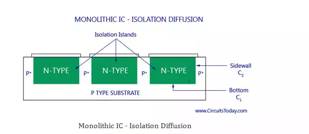
An effect of capacitance is produced in the region where the two adjoining isolation islands are connected to the P-type substrate. This is basically a parasitic capacitance that will affect the performance of the IC. This kind of capacitance is divided into two. As shown in the figure C1 is one kind of capacitance that forms from the bottom of the N-type region to the substrate and capacitance C2 from the sidewalls of the isolation islands to the P-region. The bottom component C1 is essentially due to step junction formed by epitaxial growth and, therefore, varies as the square root of the voltage V between the isolation region and substrate. The sidewall capacitance C2 is associated with a diffused graded junction and so varies as (-1/2) exponential of V. The total capacitance is of the order of a few picoFarads.
Base Diffusion
The working of base diffusion process is shown in the figure below. This process is done to create a new layer of SiO2 over the wafer. P-regions are formed under regulated environments by diffusing P-type impurities like boron. This forms the base region of an N-P-N transistor or as well as resistors, the anode of diode, and junction capacitor. In this case, the diffusion time is so controlled that the P-type impurities do not reach the substrate. The resistivity of the base layer is usually much higher than that of the isolation regions.
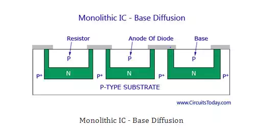
The isolation regions will have a lot lesser resistivity than that of the base layer.
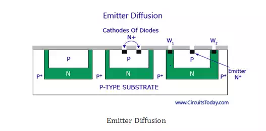
Emitter Diffusion
Masking and etching process is again carried out to form a layer of silicon dioxide over the entire surface and opening of the P-type region. The transistor emitters, the cathode regions for diodes, and junction capacitors are grown by diffusion using N-type impurities like phosphorus through the windows created through the process under controlled environmental process. As shown in the figure below there are two additional windows: W1 and W2. These windows are made in the N-region to carry an aluminium metallization process.
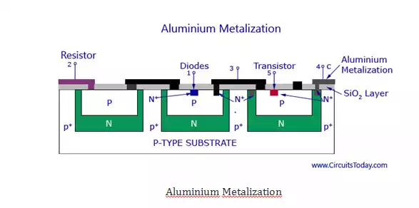
Aluminium Metallization
The windows made in the N-region after creating a silicon dioxide layer are then deposited with aluminium on the top surface. The same photoresist technique that was used in photolithographic process is also used here to etch away the unwanted aluminium areas. The structure then provides the connected strips to which the leads are attached. The process can be better understood by going through the figure below.
Scribing and Mounting
This is the final stage of the IC manufacturing process. After the metallization process, the silicon wafer is then scribed with a diamond tipped tool and separated into individual chips. Each chip is then mounted on a ceramic wafer and is attached to a suitable header. Next the package leads are connected to the IC chip by bonding of aluminium or gold wire from the terminal pad on the IC chip to the package lead. Thus the manufacturing process is complete. Thu, hundreds of IC’s is manufactured simultaneously on a single silicon wafer.