Timing Analysis
Timing analysis is the process used to verify that the timing requirements of each chip in a circuit are met. If this is not the case the circuit may operate erratically or not at all. After this lecture you should be able to draw a timing diagram for a simple circuit, derive the expressions for a chip’s timing requirements from the timing diagram and compute the margin for each requirement based on clock periods and the guaranteed responses of the other components.
Timing Specifications
A chip’s timing specifications are of two types:
(1) timing requirements and
(2) guaranteed responses.
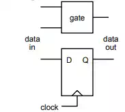
Guaranteed responses, such as propagation delays, are timing relationships between the chip’s inputs and outputs (or possibly between two outputs) that the manufacturer guarantees will always apply. Timing requirements (such as setup times) are the time relationships between a chip’s inputs that the chip’s manufacturer states are required for the chip to operate properly. The diagram below shows the simplest examples of the two types of circuits: a logic gate (an example of a combinational circuit) and a D flip-flop (an example of a sequential circuit):
and the diagram below shows the three most common timing specifications:
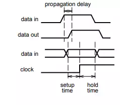
The most common guaranteed response is the propagation delay which is the maximum delay between a change in the input and the correct value appearing at the output. The most common timing requirements are the setup time and hold time which are the minimum lengths of time that the data input to a flip-flop has to be at the desired value before and after the relevant clock edge. In addition to these 3 basic specifications many chips either require or guarantee a minimum or maximum pulse width or min/max cycle time (waveform periods).
Timing Analysis :
A complete timing analysis should be part of every microcomputer system design. After a preliminary circuit design the designer should evaluate all of the timing requirements for each device and ensure that they are met. The first step in the analysis is to draw timing diagrams that show the relevant signals and specifications. This may include signals generated by clocks, by the microprocessor, by memories and by interface circuits such as address decoders and buffers. The diagrams are then used to derive expressions for the timing requirements of the devices in terms of the guaranteed timing responses of the other devices. This is done by deriving equations for the minimum (or possibly maximum) values of each requirement in terms of clock periods and/or other chip’s timing specifications. When numerical values are substituted for the values in the equations a minimum (or possibly maximum) value is obtained for that specific circuit. The difference between the computed value and the requirement is the margin. If any one of the margins is negative then the chip’s timing requirements are not met and the design must be changed. Typical changes include: adding wait states latching signals to extend them using redundant logic gates to add small delays
![]()
Timing Diagrams
Timing diagrams clarify the meanings of timing specifications by labeling the times between signal transitions using symbols from tables of timing specifications. Some conventions used in timing diagrams are: high and low levelsshown at the same time indicate the signal is fixed but can have either value (e.g. a data signal) shading between two levels indicates that the value is allowed to change a single line between the two levels indicates that the line is in high-impedance (“tri-state”) state arrows drawn between transitions on different signals show that one signal transition causes or affects another sloped transitions between levels allow references to the signal reaching a low (VOL/VIL) or high (VOH / VIH) value .It is important to understand that timing diagrams are not drawn to scale. This allows chips with different specifications to share the same timing diagram, allows small delays to be shown more clearly and also allows the same label on the diagram to refer to both maximum and minimum values. Therefore you shouldn’t necessarily rely on the timing diagram to show the order in which signal transitions happen.
Example:
As a simple but complete example, consider a simple Moore state machine:
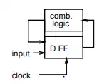
Exercise: Draw a timing diagram for this circuit. It should include the clock , the flip-flop’s input and its output, . What are the timing requirements that need to be satisfied? Assume the clock is operating at 10 MHz ( ns) and the flip-flops require a minimum setup time, , of 20ns and a minimum hold time, of 0 ns. Assume the maximum propagation delay through the combinational circuit is guaranteed to be ns and there is no minimum for . Label the timing diagram with each of these specifications. Derive expressions for each timing requirement in terms of the clock period and guaranteed timing specifications. Substitute the actual values and compute the remaining margin. Will this circuit operate properly as far as timing is concerned? What if the hold time requirement was 5 ns?