Digital system design hierarchy
Introduction
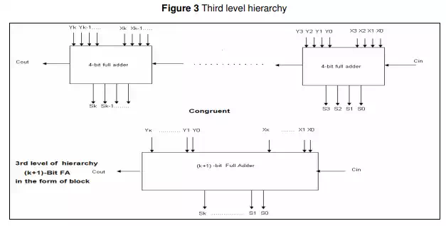
The concept of hierarchical design is essential for Computer Science and Engineering Students (CSES) to grasp as it is a significant concept in the development of software and hardware systems. The use of top down hierarchy involves dividing a module into submodules and then repeating this operation on the sub-modules until the complexity of the sub-modules has reached a suitably comprehensible level of detail [1] ( p.239). The concept of hierarchical design is used in a variety of courses included in the curricula of Computer Science and Engineering departments. In this paper, emphasis is placed on the use of bottom-up hierarchical design in hardware courses and especially in Logic Design (LD). In Logic Design, the first level of hierarchy consists of a number of Logic Gates used to implement basic Boolean functions such as 1-bit Full Adder (1FA), the whole configuration of the aforementioned logic gates creating a new entity, the ‘module’, in our example: 1FAmodule [2]. As each 1-Bit FA consists of two Half-Adders, understanding the operation of 1- Bit FA pre-supposes understanding the operation of Half-Adder in terms of its Truth-Table and its diagrammatic configuration using logic gates [2]. At the second level, the 1-bit Full Adder is used as a basic building block to construct one 4-bit Full Adder (4FA). This 4FA can easily be constructed by appropriately connecting four 1FA-modules. At the third level, a number of 4FAs could be used to construct FAs with a variable number of bits eg. 7-bit, 12- bit, 32-bit, etc. The FAs constructed at this level can be directly used as building blocks in an ALU (Arithmetic Logic Unit) in a microprocessor (MCPU).
The Context of the Study
This study focuses on the approaches of CSES to the hierarchical design used in the implementation of hardware systems, in particular the design of 11-bit Full Adder using blocks of 4FAs. This study was carried out at the Department of Computer Engineering and Informatics, Patras University, Greece. The data from this study consisted of CSES’s written documents (200 documents) from final exams taken after their participation in a onesemester course entitled ‘Logic Design I”. During this course, CSES attended lectures on the concept of digital design and hierarchical digital design, the use and operation of 1-bit and 4- bit FAs as well as blocks of 4FAs and the appropriate connection necessary to form more complicated FAs. To make better sense of the theory presented during these lectures, CSES were provided with various specific examples of hierarchical design. Students did not have any prior knowledge in the domain before entering this course. However, it is worth noting that the ratio of students to professors was about 280/1 and also that these students could sit the final exams without having attended any of the learning activities organized by the professor during the course. In fact, no more than 30% of the enrolled CSES usually participate in the class work. In addition, as the number of teaching assistants and the labrooms are limited, the related laboratory exercises are performed in the next semester.
Data analysis
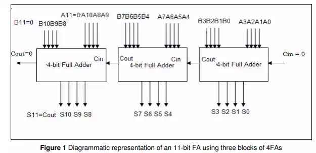
The correct solution to the given problem CSES approaches to the diagrammatic representation of a 11-bit FA using blocks of 4FA were classified, taking into account the basic steps needed to arrive at the correct solution to this problem. This step-by-step correct solution, presented in Figure 1, is as follows: A. Use of the correct number of 4FAs and connecting them appropriately: a) Use of three 4FAs, b) correct connection of these three 4FAs: this means that the Cout output of the first 4FA must be connected to the Cin input of the second FA and so on, c) for each 4FA: correct arrangement and naming of the 8 inputs which represent the two four-bit parts of numbers A and B. For example, for the first 4FA we have (3, 2, 1, 0) and (3, 2, 1, 0) as inputs for the appropriate pins, d) correct arrangement and naming of the 4 outputs which represent the summation of A and B. For the second 4FA, the outputs (S7, S6, S5, S4) are the sum of (A7, A6, A5, A4) and (B7, B6, B5, B4) plus the appropriate carry input. B. Initialization of the circuit: a) initialization of the Cin input as zero for the first 4FA, b) Initialization of A12 and B12 as zeros, c) as a result the Cout of the 11FA appears in S11 pin and the Cout of the third 4FA is always zero. C. Use of explicatory comments: Comments must be used to provide evidence for the diagrammatic solution given.
Background knowledge for the understanding of hierarchical design Understanding of hierarchical design implies understanding a 3-level hierarchy. At the first level, learners have to understand the structure of 1-Bit FA (see Figure 2a).
Figure 2 First and second level hierarchy
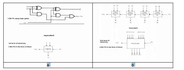
At the 2nd level, students have to understand how four 1-Bit FAs are connected to produce a block of a 4-Bit FA (see Figure 2b). At the third level, students have to understand the synthesis of (k+1)-Bit FA as a block consisting of various 4FAs (see Figure 3).