Use LTspice to Understand the LM741 OpAmp: Part 2
How op-amps work: Part 2 of 2
We left off last time
finishing up how the input stage of an op-amp works. The next important stage
is made up by transistors Q3,Q5, Q6, Q7, and Q8. The
emitters of the differential input (see Part 1) are
connected to the emitters of Q5 and Q6, this provides for level shifting, which
is required for voltage swing and DC level input at the second stage. The
current mirror load is made up of Q3,Q6, R1, and R2.
Let’s walk through this a little more.
ICQ7=ICQ8ICQ7=ICQ8
I=ICQ5=ICQ6=ICQ7=ICQ8I=ICQ5=ICQ6=ICQ7=ICQ8
ICQ3=2Iβ+VBEQ8+IR2R3=2Iβ+VTln(IIS)+IR2R3ICQ3=2Iβ+VBEQ8+IR2R3=2Iβ+VTln(IIS)+IR2R3
Hopefully, these equations
shed a little more light on the signal path and general functioning of the 741
op-amp thus far...I assure you, the input stage we completed in Part 1 is the most complicated part of this circuit.
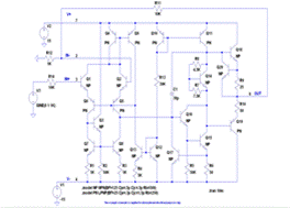
Recall the input stage:
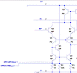
Figure 1
One more feature you may have
noticed is the offset null 1 and 2. In simulation this is not necessary to
tweak, but in real life it will be necessary to include a pot between offset
null 1 and 2. Why? Well, when there is no difference between the two inputs (Q1
and Q2) you may get a nonzero output. This is due to transistor and resistor
mismatches...nothing's perfect! To balance the mismatches and obtain a zero
output when there is no difference in input, put a pot between offset null 1
and 2 and trim it until your output looks good. To read further on the
mathematics about this, Texas Instruments has already worked out some good math
about the subject as seen here.
Now this is great and all: we
have a pretty solid input stage, things are looking up, we kind
of understand what’s going on...But wait! We have a differential input and the
741 op-amp only has one output. How do we convert the differential input to a
single ended signal? Whoa, wait a second, what? Oh don’t worry, the creator of
the 741 (David Fullagar) already thought this out for us. The
active load (Q3,Q8, R1,R2) create a modified Wilson current mirror. Its purpose is to take the differential input current and
make it a single-ended signal without the 50% loss of converting from two
signals to one. Follow? It gets a little fuzzy, I know. A small signal differential
current in Q6 versus Q5 looks summed at the base of Q16. Study the active load
schematic closely...It might take some time to absorb this concept, but you'll
get it.
Get it? Got it? Good.
Ok, now we finally can move
on from that input stage. The single-ended signal is fed to Q16. Q16 and Q15
create a Darlington configuration. That is, the current amplified by the first
transistor Q16 is subsequently amplified again by Q15. This creates a high
currentgain(
ββββ
). Q17
exists as a form of negative feedback to prevent saturation. If it gets too
high, Q17 turns on and diverts the base current going into Q16 to ground, thus
stabilizing the configuration. This amplifier uses the output side of the
current mirror created between Q10 and Q11; it is an active load. Active loads
lead to significant voltage gain because if the active load were perfect the
voltage gain would be infinite if you worked out the thevenin equivalent
resistance for a current source
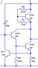
Figure 2
In figure 2, Q14 provides
a voltage level shift. The level shifter stage is included to ensure that there
is no DC offset in the output signal. DC offset arises from the turn on
voltages of the transistors throughout the circuit. As a exercise
run the simulation with and without Q14 noting the differences between the two
plots.
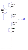
Finally we arrive at the
output stage! The output stage is composed of Q18, Q20 and Q19. The output
stage is a Class AB push pull emitter follower amplifier, go look that up if
you're not familiar with the concept. Q18 provides output current limiting much
like we saw with Q17. That’s it! Go have fun with the simulation. Play around
with it and I think it will all start coming together.
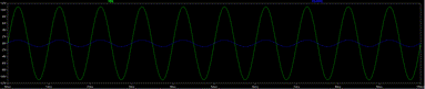
Simulating an
inverting amplifier with unity gain (click to enlarge)