Negative Feedback, Part 5: Gain Margin and Phase Margin
Use frequency-domain simulations to analyze loop gain and evaluate the stability of your amplifier circuit.
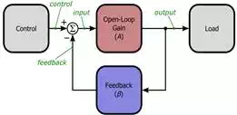
Just so you don’t have to switch pages every time you want to ponder the general feedback structure, here is the diagram presented in the first article:
In the previous article, we saw that the critical quantity in stability analysis is loop gain—i.e., the frequency response of the open-loop gain multiplied by the frequency response of the feedback network. If the magnitude of the loop gain is greater than unity at f180(i.e., the frequency at which the loop gain’s phase shift is 180°), the circuit is unstable. It would be reasonable to conclude that the circuit is stable if the magnitude of the loop gain is less than unity at f180, but real life is rarely so conveniently straightforward. As mentioned in the previous article, loop gain magnitudes slightly less than unity at f180 will lead to marginal stability, which can actually be much worse than flagrant instability. Thus, we need a way to determine whether a circuit is sufficiently stable—in other words, stable enough to ensure that the circuit will perform properly despite part-to-part variations and environmental or operational conditions that affect the characteristics of the open-loop gain or the feedback network. There is where gain margin and phase margin come into play.
Before we move on to the simulations, let’s briefly consider one important question: What if the loop gain’s phase shift never reaches 180°? Recall that each pole in a circuit’s transfer function provides 90° of phase shift. If a circuit has only one pole, no frequency component will ever be phase shifted by more than 90°, and consequently the circuit is unconditionally stable. Real-life amplifiers include various sources of parasitic capacitance and inductance, so a true one-pole response is not very practical. However, an amplifier circuit can be designed to have a dominant low-frequency pole, such that the open-loop gain resembles a one-pole response throughout most of the amplifier’s usable bandwidth; the result is an amplifier that will be stable in the vast majority of applications. Most op-amps are designed this way—these “internally compensated” op-amps sacrifice high-frequency response in favor of stability.
Once Upon a Time, Before Digi-Key Stocked 4,000 Different Op-Amps . . .
For the following simulations we will use a discrete BJT amplifier circuit. Here is the LTSpice schematic:
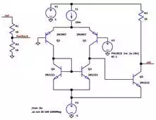
Note that you can copy the simulation commands and V3 specs if you want to quickly reproduce this simulation environment.
This simple circuit will be better for transient simulations than LTSpice’s op-amp macromodels, and it is wonderfully unstable compared to internally compensated op-amps. What you see here is essentially a simplified two-stage amplifier. Q1 and Q2 form a differential pair, with Q3 and Q4 functioning as an active load. This is the first stage. The second stage is the common-emitter amplifier consisting of Q5 and R3. The resistance of R3 is chosen so as to make Q5’s collector current similar to the value of current source I1, which in a real circuit would be implemented as a current mirror. Currently the circuit is configured for simulating the open-loop gain, because the negative input (on the left) is grounded, with the voltage source connected to the positive input (on the right). For closed-loop simulations, the negative input would be connected to the node labeled “feedback” instead of ground. R1 and R2 form the feedback network; these resistors are arranged so as to resemble a typical voltage divider, in order to emphasize the fact that the feedback factor β is the percentage (expressed as a decimal) of the output that is fed back and subtracted from the input. The values shown above—i.e., R1 = R2 = 1 kΩ—correspond to β = (1 kΩ)/(1 kΩ + 1 kΩ) = 0.5. If we decrease R1 to 100 Ω, we have β = (100 Ω)/(100 Ω + 1 kΩ) = 0.091.
First let’s take a look at the open-loop gain (magnitude is the solid-line curve, phase is the dotted-line curve):
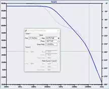
The first thing to understand is that this is not only a plot of the open-loop frequency response—it is also a plot of Aβ when β = 1. Recall that the closed-loop gain equals 1/β; thus, we can use the open-loop frequency response to determine if the circuit will be stable when it is configured for a closed-loop gain of unity. As you can see, this amplifier is seriously unstable: the magnitude of the loop gain at f180 is 25 dB. So we definitely won’t be using this amplifier as a unity-gain buffer.
Higher Closed-Loop Gain = Lower β = More Stability
Now let’s see how Aβ changes when β is less than 1. We do this by sizing R1 and R2 for the desired closed-loop gain and then telling LTSpice to plot “V(out)*(V(feedback)/V(out))” (because β = Vfeedback/Vout). Note that here we still have the circuit configured for open-loop gain (i.e., negative input terminal grounded). We are simulating open-loop gain A and then plotting A multiplied by β. Here is the loop gain for the original resistor values of R1 = R2 = 1 kΩ (and thus β = 0.5):
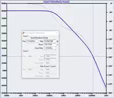
Now the gain at f180 is 19 dB instead of 25 dB. This is an improvement, but we are still far from stability. You may have noticed that the decrease in the loop gain’s magnitude is simply the dB equivalent of the closed-loop gain: GCL = 1/β = 2, and voltage ratio of 2 = 6dB. This makes sense, because when we multiply A by βwe are simply shifting the A curve according to the dB equivalent of β (remember that multiplication with ordinary numbers translates to addition with logarithmic values). In this example, β = 0.5 = -6 dB, so we shift the entire A curve downward by 6 dB. (This simple relationship is valid only when β is constant over frequency, as is essentially the case when the feedback network is composed only of resistors.)
By now you have probably realized that we don’t need to blindly experiment to determine the closed-loop gain at which the amplifier will become stable. We can readily see that a closed-loop gain of 25 dB is needed to shift the curve downward far enough to achieve unity loop gain at f180. Gain of 25 dB corresponds to a ratio of about 18 V/V, which means β = 0.056. We can obtain this β with R1 = 1 kΩ and R2= 59 Ω:
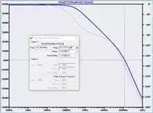
Now we have unity loop gain at f180. With a little more closed-loop gain we will have a marginally stable amplifier. How much more closed-loop gain do we need to achieve reliable stability? Consider this plot for GCL = 50 (and thus β = 0.02).
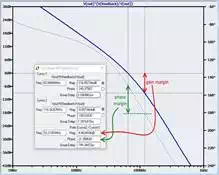
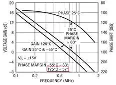
The first cursor marks the magnitude where it crosses 0 dB, and the second cursor marks the magnitude where the phase shift is 180°. Gain margin is the difference (expressed as a positive dB value) between 0 dB and |Aβ| at f180. More gain margin means more stability. Similarly, phase margin is the difference (expressed as a positive number) between 180° and the phase shift where |Aβ| crosses 0 dB. If this is still a little foggy, stare (pensively) at the above plot for a little while. The more commonly used metric is phase margin, perhaps because it comes with a handy rule of thumb: an amplifier should be designed to have a phase margin of at least 45°. More phase margin means more stability, because higher phase margin indicates that the frequency at which the loop gain magnitude reaches unity is farther away from the frequency of the dreaded 180° negative-feedback-to-positive-feedback phase shift. The following plot for the LT1001 op-amp from Linear Tech shows that the open-loop gain has been designed for a minimum phase margin of 57°, meaning that the amplifier will be thoroughly stable even when β = 1.
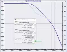
Our amplifier needs to be configured for a closed-loop gain of about 78 (β = 0.013) to achieve a phase margin of 45°:
We now know a basic approach for simulating loop gain, and we have explored the relationship between β, closed-loop gain, and stability. We also understand that phase margin can help us to decide if an amplifier is sufficiently stable. In the next article we will discuss in detail an alternative (and in some cases quite advantageous) way of using A and β to assess stability.