Understanding the
Delta-Sigma ADC
Learn more
about the Delta-Sigma ADC (analog-to-digital
converter) which relies upon oversampling and noise shaping to achieve
high-resolution conversions.
ADCs can be described as
either Nyquist-rate or oversampled converters. In my previous article, Deciphering Resolution and Sampling Rate, I explained how sampling in the
Nyquist-rate family of converters works and one of the key concepts this type
of converter relies upon, the Nyquist Criterion.
The Delta-Sigma ADC works a
little differently from the Nyquist-rate ADC. It relies upon oversampling and
noise shaping to achieve high-resolution conversions.
My previous article, Understanding the Successive Approximation Register
ADC, demonstrates a
weakness of this Nyquist-rate architecture: Its accuracy and linearity, and
thus its maximum effective resolution, are limited by the imperfections
of analog components such as the DAC.
The oversampled family of
converters, to which the Delta-Sigma ADC belongs, aims to overcome the
limitations of Nyquist-rate converters. The Delta-Sigma ADC consists of a
modulator, a filter, and a decimator as shown below. Delta-Sigma ADCs are
approximately 75% digital.
By introducing more complex
digital circuitry and oversampling the data, they attempt to reduce the
requirements for accurate analog components
that can be considered the limiting factor in other ADC architectures.

Oversampling
In order to understand the
concept of oversampling, an analysis in the frequency domain is required.
If we consider the example of
a sine wave at the input to the data converter, according to the Nyquist
Criterion, the minimum sampling frequency is defined as twice the bandwidth of
the signal.
![]()
For our example of a sine
wave, we see a peak at the frequency of interest but lots of noise, as well, as
shown below:
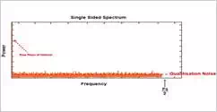
This noise is known as quantization noise (PDF) and is due to the fact that the samples of the
continuous input sine wave can only take a finite number of discrete states
determined by the resolution of the ADC. This random quantization error exists
within the Nyquist band extending up to Fs/2 and can be described as:
![]()
From this, we can determine
the signal to quantization noise ratio as:
![]()
Thus, in a Nyquist-rate ADC,
we improve the SQNR (signal-to-quantization-noise ratio) by increasing the
resolution (denoted by N) of the ADC. For a more in-depth explanation of these
formulas, please refer to my previous article, Deciphering Resolution and Sampling Rate.
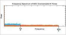
If instead we now increase
the oversampling frequency from Fs to KFs, as shown below, the quantization
noise in the region Fs/2 is reduced. The SQNR is actually the same.
The quantization noise,
however, is spread over the larger frequency range. By incorporating a filter
into Delta-Sigma ADCs, some of this quantization noise can be removed. Thus, this
reduction in quantization noise over the frequency range of interest enables
the low-resolution Delta-Sigma architecture to perform high-resolution analog-to-digital conversions.
The SQNR improves by 6 dB if
we increase the sampling rate by a factor of 4. In other words, each time we
quadruple the sampling rate, we gain the equivalent of adding 1 bit to the
resolution of the ADC. With oversampling alone, in order to achieve a 12-bit
resolution, the input must be oversampled by a factor of 411. Or, more generally, for an N-bit
increase in resolution, we must oversample by a factor 22N.
Fortunately, another
technique is used known as noise shaping to enable a gain of more than 6 dB.
Noise Shaping
The block diagram of a first
order Delta-Sigma Modulator is shown below. This consists of a difference
amplifier, an integrator, a comparator, and a switch. The switch, or 1-bit DAC,
switches a negative or positive reference voltage into the negative input of
the amplifier.
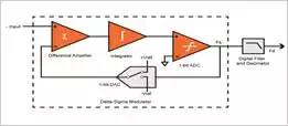
In this architecture, if the
input signal has increased, the 1-bit ADC, which is simply a comparator,
generates a one. If it has decreased, it generates a zero. As such, the
Delta-Sigma modulator transmits the changes in, or the gradient of, an input
signal.
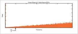
As with oversampling, noise
shaping is best explained in the frequency domain. A frequency domain model of
the modulator is shown below:
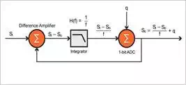
The integrator in this
architecture acts as a lowpass filter to
the input signal. Quantization noise is added to the signal output of this
filter due to the 1-bit conversion process. The output of the modulator can be represented
using the equation below.
![]()
The first term in this
equation can be considered the signal term and the second term can be
considered the noise term. As the frequency approaches zero, it can be seen
that the noise term approaches zero and the output of modulator approaches Si. As the frequency is increased, the
noise term approaches q and the signal term approaches zero. As such, the
integrator acts as a highpass filter for
the quantization noise.
Higher order Delta-Sigma
ADCs, with more than one stage of integration and summation in the modulator,
can be used to achieve further noise shaping.
Digital Filtering and Decimation
The Delta-Sigma modulator
pushes the noise to higher frequencies to increase the resolution of the ADC
and performs the conversion of the analog input
to a bit stream. The digital filtering and decimation stage are used to filter
out the high-frequency noise and reduce the data rate to a usable amount.
The filter used is most often
a type of averaging filter known as a sinc filter.
Because the noise has been pushed to high frequencies, the lowpass filter response acts to attenuate the
quantization noise. Thus, a high-resolution version of the original signal has
been obtained.
The output data rate of the
filter is the same as the sampling rate (Fs). The filter has reduced the
frequency bandwidth of the signal. As such, and according to the Nyquist
Criterion, most of the samples do not contain any useful information.
Decimation is the process of
discarding the unnecessary samples and is used as a mechanism to reduce the
data rate to a usable value whilst maintaining the information according to the
Nyquist Criterion.
The Delta-Sigma ADC has two
sampling rates, the input sampling rate (Fs) and the output data rate (Fd). The ratio of Fs to Fd is
known as the Decimation Ratio (DR). By reducing the filter’s passband and
increasing the DR, whilst maintaining the same Fs, the effective number of bits
(ENOB) for a Delta-Sigma ADC can be increased. Likewise, the bandwidth of the
ADC can be increased at the expense of ENOB.
Summary
Strengths of the Delta-Sigma ADC
● Resolution less reliant on analog components
● Extremely high resolution achievable
Weaknesses of the Delta-Sigma ADC
● Low sampling rates for high resolutions
Applications of the Delta-Sigma ADC
Delta-Sigma ADCs offer very
high resolution with an ENOB of 20-24 bits. This makes them a good choice for
precision industrial measurement applications, thermocouple temperature
measurement, and voiceband applications.