Hazards in
Combinational Logic
Learn about
hazards in combinational logic circuits
If the input of a
combinational circuit changes, unwanted switching variations may appear in the
output. These variations occur when different paths from the input to output
have different delays. If, from response to a single input change and for some
combination of propagation delay, an output momentarily goes to 0 when it
should remain a constant value of 1, the circuit is said to have a static
1-hazard. Likewise, if the output momentarily goes to 1 when it should remain
at a constant value of 0, the circuit is said to have a 0-hazard.
When an output is supposed to
change values from 0 to 1, or 1 to 0, this output may change three or more
times; if this situation were to occur, the circuit is said to have a dynamic
hazard. Figure 1.1 shows the different outputs from a circuit with hazards. In
each of the three cases, the steady-state output of the circuit is correct,
however, a switching variation appears at the circuit output when the input is
changed.
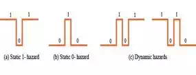
Figure 1.1
The first hazard in Figure
1.2, the static 1-hazard depicts that if A = C = 1, then F = B + B' = 1, thus the output F should remain at a
constant 1 when B changed from 1 to 0. However in the next illustration, the
static 0-hazard , if each gate has a propagation of 10 ns, E will go to 0
before D goes to 1, resulting in a momentary 0 appearing at output F. This is
also known to be a glitch caused by the 1-hazard. One should note that right
after B changes to 0, both the inverter input (B) and output (B') are 0 until
the delay has elapsed. During this propagation period, both of these input
terms in the equation for F have value of 0, so F also momentarily goes to a
value of 0.
These hazards, static and
dynamic, are completely independent of the propagation delays that exist in the
circuit. If a combinational circuit has no hazards, then it is said that for
any combination of propagation delays and for any individual input change, that
output will not have a variation in I/O value. On the contrary, if a circuit
were to contain a hazard, then there will be some combination of delays as well
as an input change for which the output in the circuit contains a transient.
This combination of delays
that produce a glitch may or may not be likely to occur in the implementation
of the circuit. In some instances it is very unlikely that such delays would
occur. The transients (or glitches) that result from static and dynamic timing
hazards very seldom cause problems in fully synchronous circuits, but they are
a major issue in asynchronous circuits (which includes nominally synchronous
circuits that involve either the use of asynchronous preset/reset
inputs that use gated clocks).
The variation in input and
output also depends on how each gate will respond to a change of input value.
In some instances, if more than one input gate changes within a short amount of
time, the gate may or may not respond to the individual input changes. One
example in Figure 1.2, assuming that the inverter (B) has a propagation delay
of 2ns instead of 10ns. Then input D and E changes reaching the output OR gate
are 2ns from each other, thus the OR gate may or
may not generate the 0 glitch.
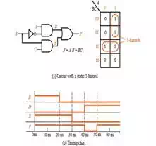
Figure 1.2
A gate displaying this type
of response is said to have what is known as an inertial delay. Rather often
the inertial delay value is presumed to be the same as the propagation delay of
the gate. When this occurs, the circuit above will respond with a 0 glitch only
for inverter propagation delays that are larger than 10ns. However, if an input
gate invariably responds to input change that has a propagation delay, is said
to have an ideal or transport delay. If the OR gate shown above has this type
of delay, than a 0 glitch would be generated for any nonzero value for the
inverter propagation delay.
Hazards can always be
discovered using a Karnaugh map. The map
illustrated above in Figure 1.2, which not a single loop covers both minterms ABC and AB'C. Thus if A = C = 1 and B's value
changes, both of these terms can go to 0 momentarily; from this momentary
change, a 0 glitch is found in F. To detect hazards in a two-level AND-OR
combinational circuit, the following procedure is completed:
A sum-of-products expression
for the circuit needs to be written out.
Each term should be plotted
on the map and looped, if possible.
If any two adjacent 1's are
not covered by the same loop, then a 1-hazard exists for the transition between
those two 1's. For any n variable map, this transition only occurs when one
variable changes value and the other n 1 variables
are held constant.
If another loop is added to
the Karnaugh map in Fig. 1.2(a) and then
add the corresponding gate to the circuit in Figure 1.3 below, the hazard can
be eliminated. The term AC remains at a constant value of 1 while B is
changing, thus a glitch cannot appear in the output. With this change, F is no
longer a minimum SOP.
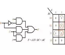
Figure 1.3
Figure 1.4(a) is a circuit
with numerous 0-hazards. The function that represents the circuit's output is:
F = (A + C)(A' + D')(B' + C' + D)
The Karnaugh map
in Fig. 1.4(b) has four pairs of adjacent 0's that are not covered by a common
loop. The arrows indicate where each 0 is not being looped, and they each
correspond to a 0-hazard. If A = 0, B = 1, D = 0, and C changes from 0 to 1,
there is a chance that a spike can appear at the output for any combination of
gate delays. lastly, Fig. 1.4(c) depicts a timing
diagram that, assumes a delay of 3ns for each individual inverter and a delay
of 5ns for each AND gate and each OR gate.
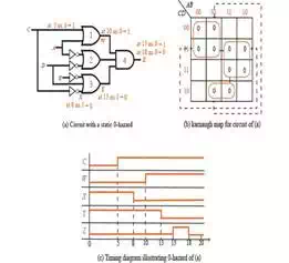
Figure 1.4
The 0-hazards can be
eliminated by looping extra prime implicants that
cover the 0's adjacent to one another, as long as they are not already covered
by a common loop. By eliminating algebraically redundant terms, or consensus
terms, the circuit can be reduced to the following equation below. Using three
additional loops will completely eliminate the 0-hazards, resulting the
following equation:
F = (A + C)(A' + D')(B' + C' + D)(C + D')(A + B' + D)(A' + B' + C')
This figure below illustrates
the Karnaugh map after removing the
0-hazards.
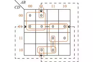
Figure 1.5
Testing of Logic Circuits
An essential component of
designing logic circuits is making sure that the final design is correct and
correcting if necessary. To test a circuit, one can either build them or
simulate them on a digital computer. Computer simulation is generally faster and
more economical because you do not have to waste money on components. As the
complexity of the circuit increases, it becomes very important to simulate a
design before actually building it. When a design is built in integrated
circuit form, it is essential to simulate because fabricating an integrated
circuit can take a very long time and correcting errors can be an expensive
fix. Simulation is done before the actual build for many reasons: confirmation
that the design is correct logically, making sure that the timing of all logic
signals are correct, and verification of faulty components in the circuit as an
aid to finding tests for the circuit.
In order to simulate a logic
circuit design, there are specific programs needed in order to build the design
on the computer. First, any components and connects to the logic inputs and
outputs need to be specified. After that, these inputs can then be specified.
Lastly, the circuit outputs should be reviewed to correct any mistakes. A
specific description of the circuit may be inputted into the computer
simulation program as to the list of any connections between logic elements, or
it may be in the form of a drawn logic diagram on the computer screen.
A simple computer simulation
program for a set of combinational logic may look like this:
The inputs of the circuit are
implemented to the first set of gates in the circuit, and the output values of
those gates are then calculated.
These outputs which changed
in the first step are then fed into the next level (or set) of gate inputs. If
any input has changed, then that same input's value is calculated.
The previous step is repeated
until there isn't a single change in gate input values. When this is met, the
circuit is said to be in steady-state condition, and finally the output values
may be read.
Steps 1-3 are repeated every
time there is a change in an input.
Coming Up
As of now, you should have an
understanding of static 0- and 1-hazards and dynamic hazards. Also, if a
combinational circuit is given, you should be able to find the hazards (both 0-
and 1-). A basic understanding should be known about
the testing and simulation of integrated logic circuits.