Combinational Circuit
Design and Simulation Using Gates
Circuit Design with Limited
Gate
Inputs
In any practical design of
logic circuits, the maximum inputs a gate (fan-in) can have is limited. This
number can vary from two, three, four, eight, or some other number, depending
on the type of gate being used in designing a circuit. If any two-level realization
of a circuit demands more gate inputs than permitted, the logic expression can
be factored to obtain a multi-level realization. Below is an example that asks
to realize
f(a,b,c,d)=∑m(0,3,4,5,8,9,10,14,15)f(a,b,c,d)=∑m(0,3,4,5,8,9,10,14,15)
by using three-input NOR gates.
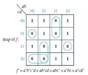
This expression is a
two-level realization; however, it requires two four-input and one five-input
gate. This requirement is not an ideal way to design any functional
combinational circuit. In order to reduce this expression, f’ is factored to
reduce the maximum number of gate inputs. After factoring this logic
expression, the number of gate inputs can be reduced to three, as shown below.
![]()
When designing a large output
circuit with more than two levels, the best technique would be to minimize each
function separately. In order to increase the number of levels, the two-level
logic expressions must be factored. When factoring, introducing common terms
wherever possible is the most ideal way to go about
simplification. Below is another example that asks to realize the
logic functions by using ONLY two-input NAND gates and inverters. Having
minimized each logic function individually, one would find:
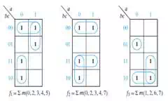
This result shows that each
logic function requires one three-input OR gate. In order to use the OR gate on
each function, reduction of gate inputs by factoring is completed below.
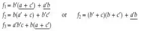
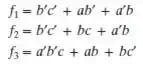
Looking closely, the logic
expression f2 has
a common term with f1 of a'b, so by using the second expression
of f2, the last three-input gate from f3 can be eliminated as shown below:
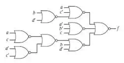
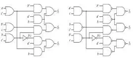
![]()
The resulting logic circuit,
having used common terms a'b and a + c',
has OR gates at each output. Converting to NAND gates is straightforward, as
shown on the right side of the figure.
Delays in Gates and Timing Diagrams
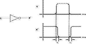
If the input of a logic gate
is changed, the output will not change instantaneously. The reason behind this
is elements that switch the inputs within the gate take a fixed time to react
to change, so the resulting change output is delayed with respect to the input.
The propagation delay in an inverter figure shown below any possible waveforms
of input and output for an inverter. For a change in output delayed by time,
εε
, taken respectfully to the input, is said to have a propagation delay of
εε
. A propagation delay for a 0 to 1 output change may be different than
that of a delay for a 1 to 0 change. Some propagation delays can be neglected
if they are as short as a few nanoseconds. However, it is good practice
to analyze these sequential circuits, no
matter how short the delay may be.
More than likely, a timing
diagram will be used to analyze sequential
circuits. Timing diagrams can be used to show different signals in a circuit as
a function of time. When plotting numerous variables, they are plotted along
the same time scale so the times at which these variables change with respect
to each other can be easily understood.
For a circuit with two gates,
as shown below, each gate is assumed to have propagation delay of 20 ns. The
diagram specifies what will happen if gate inputs B and C are held at regular
values of 1 and 0, respectively, and gate input A is changed to 1 at t = 40 ns
where it is then changed back to 0 at t = 100 ns. The gate output of G1 changes exactly 20 ns after A changes, and finally the gate output of G2 changes exactly 20 ns after G1 changes.
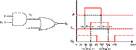
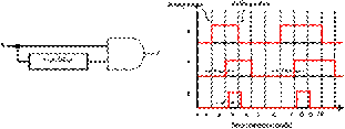
The figure below depicts a
timing diagram for a logic circuit with a delay element. Input X consists of
two pulses: the first pulse is 2 microseconds wide and the second pulse is 3
microseconds wide. The delay element that tangents off of X has output Y, which
is identical to the input, X, but it is delayed by 1 microsecond. What this
means is that Y changes from a value of 1, 1 microsecond after the rising edge
of the X pulse and then returns to a value of 0, 1 microsecond after the
falling edge of the X pulse. Z, which is the output of this AND gate, should
always be 1 during the time interval for which both X and Y have a value of 1.
Assuming that there is a small propagation delay in the AND gate of
εε
, then the output, Z, will provide the following timing diagram:
Coming Up
At this point, you should
have an understanding of how to draw a timing diagram for any combinational circuit
with and without gate delays, an understanding of designing and simplifying two
or multiple level logic circuits, as well as a full grasp on how time delays
affect gate operations. A further topic that will be explored is hazards in
combinational logic circuits, specifically finding static 0- and 1-hazards.