eMMCs: An Introduction
NAND Flash is, without a
doubt, the cheapest way to store a ton of bits in one place. It's also one of
the most aggravating memory mediums to work with. Bits wear out, errors pop up,
and data gets lost. Why deal with all the hassle of managing your memory manually?
Instead, use an eMMC!
The Trouble With NAND Flash
NAND Flash has a number of
inherent issues associated with data retention and accuracy. Failures due to
semiconductor variation can lead to data loss at any time. What's worse, these
issues are only exacerbated by time and continued use of the chip. These issues
can generally be kept at bay with a some simple
software techinques. Error correction codes,
wear leveling algorithms, and bad block
management can all extend the lifetime of a NAND chip by utilizing chip space
intelligently. However, this comes at a cost: silicon process sizes continue to
shrink following Moore's law, meaning floating gates within the chips start
becoming more vulnerable to errors. Compounding this problem is the rise of
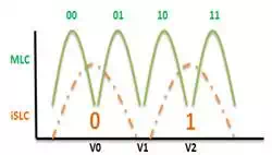
multi-level cell (MLC) and triple-level cell (TLC) NAND, which encode multiple
bit values in a single floating gate transistor! This generally means that a
more robust ECC algorithm is necessary to show data correctness, but that comes
at the cost of greater ECC bit overhead and increased computation times for
complex ECC algorithms.

(Note: I've written
previously about how NAND can break and how to prevent it from breaking in my own blog. Check it out if
you'd like to know more about NAND failure modes!)
All this complexity (and the
software written to manage it) begs the question - isn't there a better way? As
it so happens, there is!
Pick a Card, Any Card
Embedded MultiMediaCards (eMMCs for
short) grew out of the now-obsolete MultiMediaCard standard.
Though MMCs were later replaced by SD cards, the two technologies shared one
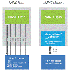
common architectural feature: instead of exposing raw NAND Flash to the host
machine, the cards contained a small controller IC that took care of processor
interfaces and chip management. The NAND management feature is a big deal -
instead of requiring the processor to do all the work of showing that nonvolatile data is good, a system processor is freed
to do other tasks! Popular but complex software workarounds, like journaling
Flash filesystems, were rendered reasonably obsolete by this development. Keep
in mind, however, that these cards are not a cure-all. They depend on Flash
memory, and thus have finite lifetimes. To help predict the health of the
internal data, most NAND vendors will expose registers to the host showing
worst-case program/erase cycles of internal blocks, as well as total P/E cycles
for the device.

Speed Freaks
The NAND management
controller within eMMCs has another benefit
over raw NAND Flash: speed. The ONFI Consoritum quotes
speeds of up to 150 MB/s in ONFI 2.0 devices; however, this is generally not
achievable in practice due to latency in address turnarounds between a
processor controller and the NAND device. The quoted maximum of most NAND is
the baseline for an average eMMC.
How do they achieve these
gains? eMMCs improve this drastically by
adopting a pipeline architecture similar to DDR DRAM - sequential reads
generally don't require additional addressing to access following sections of
memory. This is due to the availability of a cache on eMMCs that
raw NAND lacks. This onboard processor and
its cache memory allows the host processor to effectively stage data in the
controller for reading or writing into NAND cells without having to worry about
seeing those actions to completion. Thetradeoff, like
raw NAND Flash, is a hit on random read performance. Since a new location to be
read requires a staging of a page of NAND data in the controller, it is subject
to the same latency that raw NAND devices are.
A Faster Way
eMMCs offer a competitive way of
delivering robust, high performance products to the market in less time than
raw NAND solutions. They hit a real sweet spot in terms of cost, complexity,
and availability over raw NAND.
What are your experiences
designing with eMMCs? Leave us a comment and let
us know!