2N3055 Transistor Datasheet
Explored
Almost 90 % of all medium power
electronic gadgets incorporate 2N3055 transistors in their output stages –
probably enough to prove the high versatility of the device. The article
provides you with all the necessary details about this important electronic active
component.

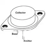
The 2N3055 is a NPN Epitaxial-Base
Planar Transistor that normally comes encapsulated in a metal Jedec TO-3 package. The basic application range
include power switching, high fidelity amplification, shunt regulation, and
forming the output stages of various power circuits.
The device has become particularly
popular due to some of its outstanding features, as summarized below:
○ Rugged design and packaging, makes it less
vulnerable to mechanical stresses during procurement and transportation.
○ High collector to emitter voltage handling
capability makes it highly versatile for most power amplification applications.
○ Low base to emitter voltage, makes it easily
switchable even with nominal output potentials available from linear ICs
without incorporating buffer stages.
○ Robust output current delivering capability
makes it ideally suited for applications in power amplifiers and power
inverters.
○ Sturdy TO-3 case encapsulation makes it
easily mountable over heat sinks with snug face to face contact, enabling
perfect heat dissipation from the device and ensuring optimum response.
○ Reasonable and consistent hFE gain makes it universally suitable and applicable
for most purposes.
○ High frequency handling range, again
attributing the device with a wide range utility feature.
○ The above versatility of the device in turn
makes it easily replaceable with other power transistors having varied
characteristics, relieving the users from the headache of searching identical
compatible matches for their individual specific applications.
Let’s have a more intense and
precise study regarding the above specialization of the device in the following
section.
2N3055 Datasheet Explained for Easy Reference
Before noting specific figures,
readers should first become familiar with the various terminologies used on the
2N3055 spec sheet. The study of the following relevant acronyms is a must for
all electronic students:
VCEO = Indicates the Collector to
Emitter Breakdown voltage of the particular device, or the maximum threshold
voltage level beyond which the device may get damaged or blown off. In simple
words for a given device, the operations must be carried out and limited below
these specified levels.
VCBO = As above,
it’s the device’s Collector to Base breakdown voltage.
VEBO = It’s the Emitter to Base
breakdown voltage.
hFE = DC Forward Current Gain or the
efficiency of the device to amplify a given signal to appreciable limits at the
collector with respect to relatively lower base biasing voltages.
IC = Collector biasing current
fT = Transition frequency or the maximum
frequency rate at which the device would operate optimally.
RƟjc = Thermal withstanding capacity from
the case junction, or the maximum allowable case temperature for the device,
above which the device might go through a thermal run-away situation to become
permanently damaged. The parameter provides the necessary data regarding the
heatsink calculations for a particularly device.
PTC = Maximum allowable
dissipation (heat) from the case at 25 degrees ambient temperature. Again, it’s
the information through which the heat sink parameters may be calculated.
The following data provides the
actual figures involved with the various 2N3055 specifications:
Polarity = NPN,
IC = 15 Amp.
VCEO = 60 Volts,
hFE = 20 (min), 70 (max) @ IC = 4 Amp, and
VCE = 4 Volts,
Safe Operating Area = 2.87 Amp ×
40 V for 1 second pulse.
fT = 2.5 MHz (min),
RƟjc = 1.52 degree C/W,
PTC = 115 Watts.
Now let’s study some of the
important and interesting practical operations associated with 2N3055
transistors.
Electronic Installation

The query regarding how to install
2N3005 would include either mechanical or electronic installations procedures,
we’ll discuss both of them here.
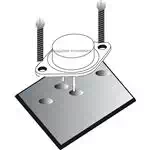
Installing or fitting 2N3055
over a heatsink: As we all
know a heatsink which is meant for absorbing heat from the device, so it needs
to be a very good conductor of heat and yet cheap. Aluminum is
the best material used for the purpose and a conventionally accepted material
as heat sinks for electronic devices. The installation of the 2N3055 would
involve the following steps:
Procure from the market or
fabricate the heat sink plate as per the specifications.
Drill holes as per the dimensions
of the transistor leads and fixing holes, as shown in the diagram.
Apply and spread some heatsink
paste over the lead side flat surface of 2N3055.
Place the component over the
drilled surface so that the leads pass through the drillings appropriately, the
fitting holes coincide with the drilled holes and the surfaces “stick"
snugly with the heatsink paste getting tightly sandwiched between the device
and the metal.
Now it’s just a matter of securing
the device by nuts and screws across the concurrent holes and tightening them
as firmly as possible.
Make sure the protruding leads
clear pass through the center of the
drillings, and is kept well aloof from the heat sink metal.
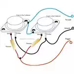
If two devices need to be fixed
over a common heatsink, then make sure the heatsink mica kit is used while
doing the above operations. However if their collectors (body) are in parallel
then they can be directly fixed over a common heatsink metal without using mica
protective insulations.
Connecting 2N3055 Transistors in Parallel

Paralleling 2N3055 Transistors
Connecting two or more 2n3055
transistors in parallel is very easy; just join their collectors and the
emitters together to produce a common terminal from the collector joint and a
common terminal from the emitter joint. The base of each transistor must also
be made common by joining, however each base terminal must incorporate the
respective resistors (usually of identical calculated values) and the free
terminal of the resistors must be joined to produce a common base connection
point (refer the diagram).
Since the body of the device forms
the collector, the respective connections must be acquired from the body
fitting screws of the transistors.
Making a Variable Power Supply Using Transistor
2N3055
Variable Voltage power Supply
Using 2N3055 Transistor
A very reliable and efficient
variable voltage and variable current power supply design can be built using a
2N3055 transistor in conjunction with a couple of other active and passive
components.
The entire explanation and diagram
has been already discussed in one of my previous posts; you can learn more
about it HERE. Though T1 in the diagram shows a TIP 33
transistor, it can be easily replaced by a 2N3055 transistor, which will also
make the circuit capable of handling higher loads.