Understanding Inductor
Designs for Converters
A demonstration of filter inductor design
for boost converters, design of the coupled inductor for a two-output forward
converter, and the design of flyback transformer
in continuous conduction mode.
The filter inductor in the
converter circuit is operated in a small B-H loop region as compared to the
wide region for the conventional transformer. The area of B-H loop is
proportional to the total current ripple in the inductor. The core losses are
negligible, according to the minor B-H loop area. On the other hand, copper
loss depends on the DC current flowing through inductor. The same curve is also
applicable in the case of coupled inductor. Design is majorly constrained by
the copper loss and the saturation condition of the filter inductor.
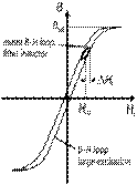
Figure 1. B-H
Loop for Filter Inductor
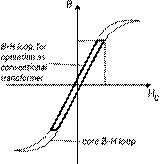
Figure 2. B-H
loop for the Conventional Transformer
Design of an Inductor for Boost Converter
The circuit diagram of the
boost converter with related waveform under CCM:
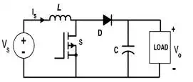
Figure 3.
Circuit of Boost Converter
The basic constraints for the
design of an inductor are (a) keep the flux density B below the flux density at
the saturation BSAT (b) keep the temperature of the inductor within limit. We also
want the inductor current ripples to be equal to the ∈
part of the inductor current.(Ripples in the Inductor
<< Inductor Current)
We should know the
requirements for this converter circuit according to the following given
specifications:
VS, VO, f, PO
Where,
VS = Input Voltage
VO = Output Voltage
f
= Operating frequency in kHz. (f=1T)
PO = Output power in kW
We can get the duty ratio of
the boost converter by this equation:
D=VO−VSVOD=VO−VSVO
The input DC current of the
converter is the inductor current which is given by this equation:
IL=IS=IO1−D=POVO1−DIL=IS=IO1−D=POVO1−D
We have seen earlier that,
Imin=DVSR(1−D)2−VS2LDT=Iavg−∆ILImin=DVSR(1−D)2−VS2LDT=Iavg−∆IL
Imax=DVSR(1−D)2+VS2LDT=Iavg+∆ILImax=DVSR(1−D)2+VS2LDT=Iavg+∆IL
Thus,
∆IL=VS2LDT∆IL=VS2LDT
[Equation
1]
Also,
∆IL=∈IL∆IL=∈IL
[Equation
2]
Thus, the required inductance
value from Equations 1 and 2 is given by
L=VSDT2∈ILL=VSDT2∈IL
R.M.S value of the inductor
current in the case of a triangular wave is given by the following expression:
(ILrms)2=(Iavg)2+112(Ipp)2=(Iin)2+112(∆I)2(ILrms)2=(Iavg)2+112(Ipp)2=(Iin)2+112(∆I)2
⇒ILrms=(ILdc)2+112(2∆IL)2−−−−−−−−−−−−−−−−−√⇒ILrms=(ILdc)2+112(2∆IL)2
R.M.S value of voltage across
inductor is given by
VLrms=DVS2+(1−D)(VO−VS)2−−−−−−−−−−−−−−−−−−−−−√VLrms=DVS2+(1−D)(VO−VS)2
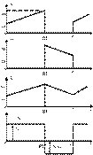
Figure 4. Supply
Current, Diode Current, Inductor Current and Inductor Voltage respectively
(Boost Converter)
If the frequency of the
converter is not less than the apparent frequency obtained from the following
expressions, it is a worst-case frequency.
fapparent=VLrms2πLfapparent=VLrms2πL
is valid for the low-frequency range under low eddy
current losses and d<1.6δ. Consider the fill factor FC according to the
type of conductor (round wire or litz wire).
Now, we have all the input parameters in designing an inductor. We can
determine the core parameters AC', AW, and lmeanT using the constraint
equations below.
NIm≈BmAC′Rg=BmAC′lgμONIm≈BmAC′Rg=BmAC′lgμO
Rw=ρlwrAC=ρNlmeanTACRw=ρlwrAC=ρNlmeanTAC
L=N2Rg=µOAC′N2lgL=N2Rg=µOAC′N2lg
FCAW≈NACFCAW≈NAC
We will then get the required
final volume of the core. We can now also multiply the volume with the
corresponding power density of the material at a particular frequency to
measure core loss. Power density is measured by the plot between the power
density at a particular frequency and the change in the magnetic flux density
given by the manufacturer. Change in flux density is given by:
∆B=VLN1AC′(DT)∆B=VLN1AC′(DT)
We can neglect the core loss
if it is comparatively less than the copper loss, and use the material which
has higher core loss and high saturation flux density. This leads to a smaller
size inductor core.
Design of a Coupled Inductor for a
Two-Output Forward Converter
Coupled inductors have
multiple windings wound on the same core for high value of inductance in common
mode current while low value of inductance for the differential mode current.
Coupled inductors have lower leakage inductance and AC current losses. Consider
a coupled inductor as shown in the figure below:
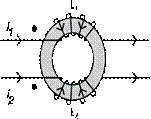
Figure 5.
Coupled Inductor
The number of turns for L1and L2 must be same to maintain the volt-time balance condition.
Magnetizing field is produced by the sum of the currents i.e. i1+i2 which flows through the core. Leakage field is produced by the
difference of the currents i.e. i1-i2 which flows through
air. The circuit diagram for the two-output forward converter using
coupled inductor is given below.

Figure 6.
Circuit for the Two-Output Forward Converter
Common Mode Current,
ic=i1+i22ic=i1+i22
Differential Mode Current,
id=i1−i22id=i1−i22
These currents both
contribute in the eddy current losses.
Common Mode Inductance,
Lc=N2Rm=PmN2Lc=N2Rm=PmN2
Differential Mode Inductance,
Ld=N2RO=PON2Ld=N2RO=PON2
Here, Pis the permeance provided
by the manufacturer and R is the reluctance. For common mode current, coupled
inductors act like two inductors L1and L2 in parallel. For differential
mode, coupled inductors act like a transformer. There is a considerable DC
component in the current flowing through L1and L2 which causes the net magnetization
of the core.
H(t)=N1i1(t)+N2i2(t)lCRmRm+ROH(t)=N1i1(t)+N2i2(t)lCRmRm+RO
Similar design procedure with
the single-winding filter inductor is used.
Design of a Flyback Transformer
in CCM
The flyback transformer
acts as an inductor, having two windings where only one of its windings carries
the current at a particular time. The flyback transformer
stores the energy and releases it later, which requires an air gap. As both the
windings carry the current alternatively even with the continuous total
ampere-turns, high AC winding losses are associated with the flyback converter irrespective of its operating
mode. Core loss depends on the magnetizing current Im for the transformer and is usually significant in the
case of the discontinuous conduction mode.
In CCM, conversion ratio for
the converter is:
VOVS=D1−D.VOVS=D1−D.
For the desired duty cycle
and nominal supply voltage, the initially expected turns ratio
is given by:
n=vsvo′D1−D=N1N2n=vsvo′D1−D=N1N2
where vo' is the sum of the voltages across
the load, switch, rectifier and copper loss referred to the secondary side. We
even need to see the duty ratio for the worst-case current of the DC and AC
components. Duty cycle and turns ratio can be possibly altered to optimize the
design. We can select the particular material according to the proper
specifications with the help of the data sheet.
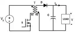
Figure 7.
Circuit for Flyback Converter
Core loss is negligible and
flux density is restricted by the saturation of the core. Net field in the core
is the sum of the magnetizing current and the leakage field. Magnetizing field
is used for the storage of energy and basically acts as an inductor while the
leakage field performs like a transformer.
Bn(t)=Bm(t)+Bl(t)Bn(t)=Bm(t)+Bl(t)
Change in Magnetic flux
density can obtained by
∆Bm=Bm∆ImIsc∆Bm=Bm∆ImIsc
Here, Isc is the short-circuit current
which produces the maximum flux density.
The number of turns on the
secondary side is given by
Ns=L∆Im∆BmAcNs=L∆Im∆BmAc
Thus, the corresponding turns
for the secondary can be calculated. Select the core shape and its type using
the guide provided by the manufacturer. Based on that, we need to calculate the
thermal resistance, conductor size, air gap length, winding loss, DC and AC
losses consequently.
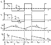
Figure 8.
Waveforms of Input Voltage, Output Voltage, Magnetizing Current, and Diode
Current for the Flyback Converter