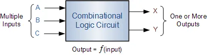
Combinational Logic Circuits
Combinational Logic Circuits are memoryless digital logic circuits whose output at any instant in time depends only on the combination of its inputs
Unlike Sequential Logic Circuits whose outputs are dependant on both their present inputs and their previous output state giving them some form of Memory. The outputs of Combinational Logic Circuits are only determined by the logical function of their current input state, logic “0” or logic “1”, at any given instant in time.
The result is that combinational logic circuits have no feedback, and any changes to the signals being applied to their inputs will immediately have an effect at the output. In other words, in a Combinational Logic Circuit, the output is dependant at all times on the combination of its inputs. Thus a combinational circuit is memoryless.
So if one of its inputs condition changes state, from 0-1 or 1-0, so too will the resulting output as by default combinational logic circuits have “no memory”, “timing” or “feedback loops” within their design.
Combinational Logic Circuits are made up from basic logic NAND, NOR or NOT gates that are “combined” or connected together to produce more complicated switching circuits. These logic gates are the building blocks of combinational logic circuits. An example of a combinational circuit is a decoder, which converts the binary code data present at its input into a number of different output lines, one at a time producing an equivalent decimal code at its output.
Combinational logic circuits can be very simple or very complicated and any combinational circuit can be implemented with only NAND and NOR gates as these are classed as “universal” gates.
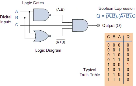
The three main ways of specifying the function of a combinational logic circuit are:
· 1. Boolean Algebra – This forms the algebraic expression showing the operation of the logic circuit for each input variable either True or False that results in a logic “1” output.
· 2. Truth Table – A truth table defines the function of a logic gate by providing a concise list that shows all the output states in tabular form for each possible combination of input variable that the gate could encounter.
· 3. Logic Diagram – This is a graphical representation of a logic circuit that shows the wiring and connections of each individual logic gate, represented by a specific graphical symbol, that implements the logic circuit.
and all three of these logic circuit representations are shown below.
As combinational logic circuits are made up from individual logic gates only, they can also be considered as “decision making circuits” and combinational logic is about combining logic gates together to process two or more signals in order to produce at least one output signal according to the logical function of each logic gate. Common combinational circuits made up from individual logic gates that carry out a desired application include Multiplexers, De-multiplexers, Encoders, Decoders, Full and Half Adders etc.