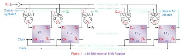
Bidirectional Shift Register
Bidirectional shift registers are the storage devices which are capable of shifting the data either right or left depending on the mode selected. Figure 1 shows an n-bit bidirectional shift register with serial data loading and retrieval capacity. Initially all the flip-flops in the register are reset by driving their clear pins high. Next R/LÌ… control line is made either low or high in order to opt for either left-shift or right-shift of the data bits, respectively.
Now if R/L̅ = 1, then A1 gates of all the combinational circuits get activated while the A2 gates will get disabled at the same time. Due to this, the outputs of each flip-flop appear at the inputs of the very-next flip-flop via OR gate output (except for the last flip-flop FFn).
For example, Q1 appears at D2 via the output of OR gate 1 (O1), Q2 appears at D3 via the output of OR gate 2 (O2), … and Qn-1 appears at Dn via the output of OR gate 1 (On) (red lines). At this instant if the positive edge of the clock pulse appears, then the outputs of the respective flip-flops reflect their inputs. Thus Q1 = D1, Q2 = Q1,… and Qn = Qn-1. This is nothing but right-shift of the data by a single bit within the register. Following on the same grounds, one can note that for every rising edge of the clock, the data within the register shifts right by a single bit as long as R/L̅ remains high.
On the other hand, if R/L̅ goes low, then A2 gates of the combinational circuits get enabled while A1 gates get deactivated. This causes the outputs of each flip-flop to appear at the input pins of the very-previous flip-flop through their OR gate outputs (except the first flip-flop, FF1). For example, Qn appears at Dn-1 through the output of OR gate n-1 (On-1), … Q3 appears at D2 via the output of OR gate 2 (O2), and Q2 appears at D1 via the output of OR gate 1 (O1). These input bits are latched onto their respective output pins as soon as the leading edge of the clock pulse appears and thus Qn-1 = Qn, …Q2 = Q3 and Q1 = Q2 (green lines). This means that for every clock tick, the data within the register moves left by one bit, provided R/L̅ line is zero.
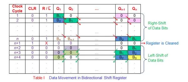
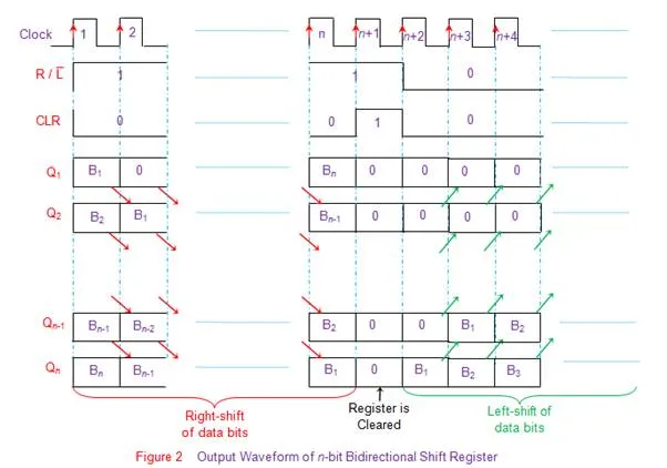
The working of such bidirectional register can be summarized as in Table I and can be further explained by the output wave forms shown by Figure 2.