Conversion of Flip-flops
Flip-flops are the basic building blocks of Sequential Circuits which can be converted from one form to another capable of storing a single bit of data
As flip-flops are bistable devices, these sequential circuits are sometimes called “latches” because their outputs are locked or latched onto their input state until there is another change to its input condition.
We have also seen that the bistable flip-flop is the most basic storage element in a sequential logic circuit and can be configured to produce simple memory elements by interconnecting two inverting gates to generate feedback. Note that a combinational logic circuit does not require any form of memory and therefore does not use flip-flops. However, sequential logic circuits do have memory and therefore use various types of flip-flop designs to remember their present states.
The interconnection of digital logic gates to produce a memory device leads to applications such as switch debounce circuits, shift registers and counters, etc. Also, memory elements made from bistable latches form the basis of accumulators and registers on which a computer, or micro-controller, does its complex arithmetic.
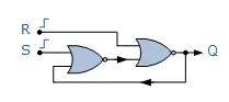
The most basic way to create a single one-bit flip-flop is to use two NOR gates gates as shown. By using cross-coupled gates and feeding the output from one gate to the input of the other, (inputs-outputs interchanged) the circuit has a closed-loop (positive feedback) so its output depends on the state of the inputs, making the circuit sequential and having memory.
Flip-flops also belong to a category of digital switching circuits called Multivibrators. The basic bistable multivibrator is a type of regenerative circuit that has two active digital gates designed so that when one digital gate conducts, the other gate is cut-off and vice versa. These two digital gates produce two stable outputs both HIGH and LOW in which one is the complement of the other.
But we can make many different types of flip-flop circuits both asynchronous and synchronous (an asynchronous flip-flop does not require a clock signal input, but a synchronous one does) from either basic cross-coupled NAND Gates and NOR Gates with the conversion of flip-flops between the different types sometimes a bit confusion.
There are basically four different types of flip flops and these are:
· 1. Set-Reset (SR) flip-flop or Latch
· 2. JK flip-flop
· 3. D (Data or Delay) flip-flop
· 4. T (Toggle) flip-flop
So to help us understand better the different types of flip-flops available, the following sequential logic tutorial shows us how we can make the conversion of flip-flops from one type to another simply by modifying the inputs of a particular type of a flip-flop starting with the SR flip-flop.
The most basic of all the bistable latches and bistable multivibrators is the set-rest (SR) flip-flop. The basic SR flip-flop is an important bistable circuit because all the other types of flip-flop are built from it. The SR flip-flop is constructed using two cross-coupled digital NAND gates such as the TTL 74LS00, or two cross-coupled digital NOR gates such as the TTL 74LS02.
Generally SR bistables and flip-flops are said to be transparent because their outputs change or respond immediately to changes in their inputs. Also since they consist of digital logic gates along with feedback, SR flip-flops are regarded as asynchronous sequential logic circuits.
The basic SR flip-flop has two inputs S (set) and R (reset) and two outputs Q and Q with one of these outputs being the complement of the other. Then the SR flip-flop is a two-input, two-output device. Consider the circuits below.
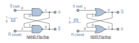
Above are the two basic configurations for the asynchronous SR bistable flip-flop using either a negative input NAND gate, or a positive input NOR gate. For the SR bistable latch using two cross-coupled NAND gates operates with both inputs normally HIGH at logic level “1”.
The application of a LOW at logic level “0” to the S input with R held HIGH causes output Q to go HIGH, setting the latch. Likewise, a logic level “0” on the R input with input S held HIGH causes the Q output to go LOW, resetting the latch. For the SR NAND gate latch, the condition of S = R = 0 is forbidden.
For the conversion of flip-flops using two cross-coupled NOR gates, when the output Q = 1 and Q = 0, the bistable latch is said to be in the Set state. When Q = 0 and Q = 1, the NOR gate latch is said to be in its Reset state. Then we can see that the operation of the NOR and NAND gate flip-flops are basically just the complements of each other.
The implementation of an SR flip-flop using two cross-coupled NAND gates requires LOW inputs. However, we can convert the operation of a NAND SR flip-flop to operate in the same manner as the NOR gate implementation with active HIGH (positive logic) inputs by using inverters, (NOT Gates) within the basic bistable design.
Then the conversion of flip-flops from active LOW to active HIGH inputs is given as:

The basic SR flip flop above and its active HIGH equivalents, are all asynchronous type flip-flops, meaning that its inputs and present state alone determine the next state. But as one-bit memory storage device we may want it to hold its current output state regardless of what’s happening to its two inputs and the operation of the basic SR flip-flop can be modified by including an additional input to control the behaviour of the bistable circuit.
The conversion of flip-flops basic circuit is achieved by using two additional AND gates which along with a control input, enable and disable the S and R inputs. This new circuit is called a Clocked or Gated SR flip-flop.
Gated SR flip-flops operate sequentially with its output state only changing in response to its inputs on the application of a clock or enable input. As the change to the output is controlled by this clock enable input, the gated SR flip-flop circuit is said to be a “synchronous” flip-flop. Then an asynchronous SR flip-flop requires no clock, but a synchronous one does.
The conversion of a standard NOR based SR flip-flop to a gated SR flip-flop is achieved using two AND gates (TTL 74LS08) connected to the Set and Reset inputs. An additional control or “Enable” input, EN is connected to both AND gates, resulting in LOW outputs when the clock input is LOW as shown.
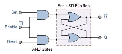
The clock or enable input, EN is connected to one of the inputs of both of the two ANDgates, resulting in LOW outputs when the enable input is LOW (AND gate principals). Then any changes to inputs S or R has no affect on the state of the outputs, Q and Q of the flip-flop.
When the enable input is HIGH the two AND gates become transparent so any changes to the inputs S and R will change the state of the outputs as before. Then we can see that either a logic level “1” (HIGH) or a “0” (LOW) can be stored at the outputs of the gated flip-flop simply by applying a HIGH to the clock enable input, and that this output state can be retained for any desired period of time regardless of the condition of the inputs while the enable input remains LOW.
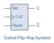
As the gated SR flip-flop is a three input device, the logic symbol shows three inputs: S, R and EN. The EN input is marked with a small triangle to denote the fact that the flip-flop responds to an edge or transition input.
The conversion of flip-flops to a clocked one is achieved by simply connecting this enable input to a timing signal. Any changes in the output state will occur in synchronisation with the clock CLK signal. Note that a clock signal is defined as a sequence of continuous pulses with each pulse having two separate states, the “ON” state and the “OFF” state, with its duty cycle representing its “ON” time divided by the total time period of pulse, (“ON” time + “OFF” time). Nearly all digital clock signals have a 50% duty cycle.
A clocked SR flip-flop can change state either on the rising positive-edge or on the falling negative-edge of the clock signal, or pulse. Therefore an edge-triggered flip-flop only responds or changes state when the clock pulse changes from one level to another. For example, HIGH to LOW or LOW to HIGH.
The output of a positive-edge triggered flip-flop only changes state on the rising edge (0-to-1) of the clock pulse and does not respond to the falling negative-edge. Likewise, a negative-edge triggered flip-flop changes state on the falling edge (1-to-0) of the clock pulse and does not respond to the rising positive-edge.
We can take this gated SR flip-flop circuit one step further to produce a bistable latch with additional inputs called Preset and Clear inputs which can be used to set a flip-flop to an initial state independent of the clock. Instead of the outputs Q and Q being loaded with an undefined value, we can over-ride all the inputs and preset the outputs to a defined state.
But why would we want to do that. Well when power is first applied to a flip-flop circuit, the initial logical state of the outputs can be completely random depending upon which logic gate latched first, then we would have no idea which switching state the flip-flop circuit is in. Therefore the initial state of the flip-flop would be uncertain as it may be in the SET state, (Q = 1) or it may be in the RESET state, (Q = 0).
Obviously this uncertainty in its switching is undesired as in the majority of applications we require the output to be set in a predefined state, either SET or RESET ready to accept data. But we can overcome this uncertainty with the conversion of flip-flops using two additional asynchronous inputs referred to as Preset, PR and Clear, CLR as shown.
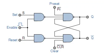
These additional inputs allow the flip-flop to be cleared, (Q = 0) whenever the CLEAR input is “0”, and the PRESET input is “1”. Likewise, the flip-flop can be preset to the logic “1” state whenever the PRESET input is “0” and the CLEAR input is “1”. In this example, if the PRESET and CLEAR inputs are active HIGH (P = CLR = 1) then the circuit operates as a normal gated SR flip-flop circuit. Clearly both the PRESET and CLEAR inputs should not be made active LOW (P = C = 0) at the same time since this leads to an uncertain state.
This PRESET and CLEAR option is also handy to have if we want to put the flip-flop into a known set or reset state during a sequential operation ready for the next sequence.
The conversion of flip-flops from one type to another is easily implemented by either modifying the connections or using additional gates. As we have seen, the basic SR flip-flop has two inputs, S and R to store a single bit but to do this we must activate both of these inputs simultaneously. Moreover, the forbidden input combination of: S = R = 1 may occur accidentally, thus causing the SR flip-flop to switch into an undefined state.
To eliminate the need for two separate inputs and the possibility of the unintentional switching into an indeterminate state, by connecting an inverter (NOT gate) between the Set and Reset inputs, we can convert the basic RS flip-flop into a D-type flip-flop.
The D-type flip-flop or Data Latch has only one input referred to as the “D”, or data input, plus a clock input, CLK along with the usual two outputs, Q and Q. The D-type flip-flop transfers its digital data between the input and its outputs, after a delay of one clock pulse and so the “D” part is also referred to as a “delay” input.
D-type flip-flops are easily constructed from an SR flip-flop by simply connecting an inverter between the S and the R inputs so that the input to the inverter is connected to the S input and the output of the inverter is connected to the S input as shown.
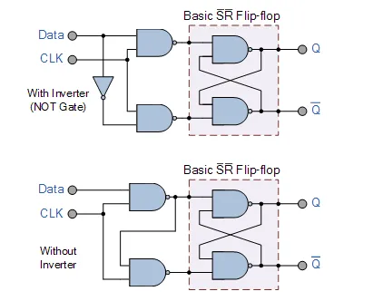
Two different circuits for the conversion of flip-flops to a D-type are given above. The top circuit is the traditional gated D-type configuration with the additional inverter. The bottom circuit functions in exactly the same manner but without the inverter, saving on one gate. As with all flip-flop configurations, D-type flip-flops can be implemented using NAND or NOR gates with or without the additional preset and clear.
The use of an inverter between the inputs ensures that the S and the R inputs are always a complement to each other eliminating the undefined condition of: S = R = 1. As a result, the D-type flip-flop is also known as a “transparent latch” as the output Q follows the Dinput when the clock input is HIGH, CLK = 1 transferring the binary information at the input directly to the output as if the flip-flop were not there, making it transparent.
The JK flip-flop is very similar in many ways to the previous SR flip-flop and is probably the most used of all the flip-flop designs. The terms “J” and “K” do not really mean or relate to any special description but where originally used at the time of the flip-flops initial development because these two letters are not used as part of any other digital device. For the JK flip-flop, the “J” is equivalent to Set and the “K” is equivalent to Reset.
We saw previously that the SR flip-flop has two or possibly three meaningful input combinations with the input sequence of S = R = 1 combination is not allowed but it can easily be modified to achieve different switching functions. Then the JK flip-flop is often considered to be a universal device.
The JK flip-flop has two inputs “J” and “K” so all four possible input configurations of: no change, set, reset and toggle are valid. With the “J” input acting like the “S” and the “K” input acting like the “R”, it changes state when one of its inputs is HIGH. However, the beauty of the JK flip-flop is that when both “J” and “K” are HIGH at logic “1”, the flip-flop toggles, that is changes from “0” to “1” or from “1” to “0” producing its own complement state.

The conversion of flip-flops to a JK flip-flop is to cross connect the Q and Q outputs with the S and R inputs through additional 3-input AND gates as shown.
If the J and K inputs are both HIGH, logic “1” then the Q output will change state (Toggle) for as long as the clock input, (CLK) is HIGH. Thus the output will be unstable creating a race-around problem with this basic JK circuit. This problem is avoided by ensuring that the clock input is at logic “1” only for a very short time, or to produce a more sophisticated JK flip-flop circuit called a Master–slave flip-flop.
The conversion of flip-flops to a “Master-Slave” configuration involves the addition of a second bistable circuit. The master-slave configuration consists of two SR latches connected in cascade. One bistable flip-flop acts as the master receiving the external inputs while the other acts as its slave, taking its inputs directly from the master flip-flop as shown.
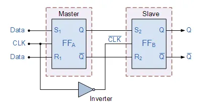
When the clock, CLK pulse goes HIGH, the data at the S and R inputs are transmitted through the master flip-flop, FFA as normal. The adjoining slave flip-flop, FFB however remains isolated since its clock input, CLK is LOW, logic “0” due to the inversion by the inverter.
Now when the initial clock pulse returns LOW to “0”, the master becomes disabled and blocks the external data inputs from passing information to its outputs, whereas the slave flip-flop now becomes enabled and thus passes the latched information to its outputs at Qand Q. Then the clock input to the slave flip-flop is the complement of the clock input to the master flip-flop.
Master–slave flip-flops are referred to as level-triggered or pulse-triggered bistable because the input data is read during the entire time that the input clock pulse is at a HIGH level. Also, master-slave flip-flops are not restricted to SR master-slave only. There are JK master-slave and D-type master-slave flip-flops as well. In nearly all of them the slave flip-flop is a standard SR flip-flop, whereas the type of flip-flop takes its name from the master part which will be SR, JK or D-type configuration.
The T-type (toggle) flip-flop is a single input bistable, with an operation similar to the D-type above. We saw above with the JK flip-flop configuration, that if J = K = 1 its output would toggle on the application of the next clock cycle. Then the conversion of flip-flops to a Toggle type is simply a matter of connecting the inputs HIGH.
The T-type flip-flop is not available commercially but can be constructed from a JK flip-flop (or D-type flip-flop) by connecting the J input with the K input and both to logic level “1”. With J and K HIGH, the flip-flop changes state every time it is triggered at its clock input. This clock input is now called the “toggle input” as the output becomes “1” if it was “0”, and a “0” if it was “1”, that is it toggles.
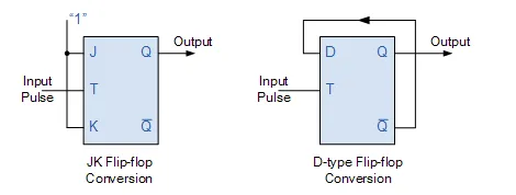
The toggle flip-flop changes state when the clock input is applied, T = 1 and remains unchanged when T = 0. Then the transition from “0” to “1” will cause the output to toggle giving the flip-flop its name. The toggle T-type flip-flop is the basic building block of many digital circuits including frequency dividers and digital counters.
Toggle T-type flip-flops can be constructed from a JK flip-flop in two simple ways. In the first is that the J and K inputs can be tied together HIGH as shown with the clock input becoming the toggle as shown. The second way is with the J and K inputs tied together to provide the toggle input with the clock input remaining unchanged. The output toggles when T and CLK= or equal to “1”. The output remains unchanged when T or CLK are LOW.
The Data D-type flip-flop can just like the JK flip-flop be converted to perform as a toggle flip-flop by connecting the Q output directly to the D-input with the toggling signal Tbeing the clock input as shown above. Connecting the Q to the input creates negative feedback.
As the output from the toggle flip-flop changes state on every application of a clock signal, its output frequency is therefore one-half that of the input signal frequency thereby acting as a frequency divider. If more toggle flip-flops are cascaded together to form a chain, as the output of the first flip-flop acts as the clock for the second T flip-flop in the cascade arrangement, and the second flip-flop acts as the clock input for the third T flip-flop, etc, creating a frequency division along the chain.
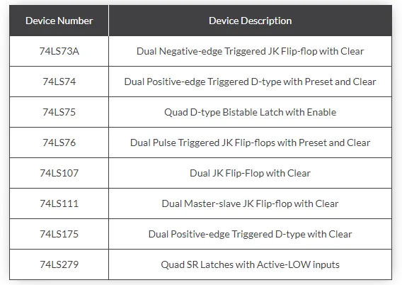
Flip-flops and latches are by far the most fundamental building block of sequential logic circuits. Therefore, many IC manufacturers produce a wide variety of different flip-flop chips that use both the TTL and CMOS technologies as listed below.
We have seen in this tutorial that a Bistable device is one in which two well defined states exist, and at any time the device could assume either of the stable states. The conversion of flip-flops from one type to another can be accomplished very easily as only slight modifications are required to convert one type to another. Flip-flops can be constructed using logic gate circuits with feedback.
We have also seen that flip-flops can have one, two or three inputs with one of those inputs connected to a clock signal. All flip-flops have two output states: Q = 1 and Q = 0which changes in response to the application of the clock. For the SR latch, S = 1 sets Q to 1, and R = 1 resets Q to 0.
The JK flip-flop is classed as a universal flip-flop and similar in design to the SR flip-flop in that when J = 1 it sets Q to 1, and when K = 1 it resets Q to 0. The condition J = K = 1causes Q to toggle.
All the flip-flops discussed above can have additional asynchronous CLEAR and PRESET inputs that cause Q to be cleared to a “0” or preset to a “1” independently of the clock signal.
A D-type bistable can be construction from JK flip-flops by the addition of an inverter between the J and K inputs. The D-type flip-flop is widely used in digital systems for transferring data and is said to be transparent, because any change in input is immediately accepted and the output changes accordingly.
The T or toggle flip-flop changes state on the application of a clock pulse when T = 1, otherwise Q does not change. The toggle flip-flop is normally used for frequency division or for designing binary counters since binary counters require complementation. The toggle flip-flop is not commercially available but can be implemented by connecting the Jand K inputs of a JK flip-flop together.
The conversion of flip-flops from one type to another is usually possible by reconfiguring the inputs, or by adding additional logic gates and we have seen that SR flip-flops can be converted to JK flip-flops which themselves can be converted to Data latches, and both the JK flip-flop and the D-type can be converted to a T-type toggle flip-flop.