Logic NOT Gate
The Logic NOT Gate is the most basic of all the logical gates and is often referred to as an Inverting Buffer or simply an Inverter
Inverting NOT gates are single input devicse which have an output level that is normally at logic level “1” and goes “LOW” to a logic level “0” when its single input is at logic level “1”, in other words it “inverts” (complements) its input signal. The output from a NOT gate only returns “HIGH” again when its input is at logic level “0” giving us the Boolean expression of: A = Q.
Then we can define the operation of a single input digital logic NOT gate as being:
“If A is NOT true, then Q is true”
A simple 2-input logic NOT gate can be constructed using a RTL Resistor-transistor switches as shown below with the input connected directly to the transistor base. The transistor must be saturated “ON” for an inverted output “OFF” at Q.

Logic NOT Gates are available using digital circuits to produce the desired logical function. The standard NOT gate is given a symbol whose shape is of a triangle pointing to the right with a circle at its end. This circle is known as an “inversion bubble” and is used in NOT, NAND and NOR symbols at their output to represent the logical operation of the NOT function. This bubble denotes a signal inversion (complementation) of the signal and can be present on either or both the output and/or the input terminals.
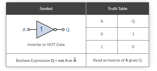
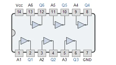
Logic NOT gates provide the complement of their input signal and are so called because when their input signal is “HIGH” their output state will NOT be “HIGH”. Likewise, when their input signal is “LOW” their output state will NOT be “LOW”. As they are single input devices, logic NOT gates are not normally classed as “decision” making devices or even as a gate, such as the AND or OR gates which have two or more logic inputs. Commercial available NOT gates IC’s are available in either 4 or 6 individual gates within a single IC package.
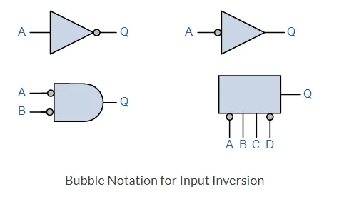
The “bubble” (o) present at the end of the NOT gate symbol above denotes a signal inversion (complementation) of the output signal. But this bubble can also be present at the gates input to indicate an active-LOW input. This inversion of the input signal is not restricted to the NOT gate only but can be used on any digital circuit or gate as shown with the operation of inversion being exactly the same whether on the input or output terminal. The easiest way is to think of the bubble as simply an inverter.
An Inverter or logic NOT gate can also be made using standard NAND and NOR gates by connecting together ALL their inputs to a common input signal for example.

A very simple inverter can also be made using just a single stage transistor switching circuit as shown.
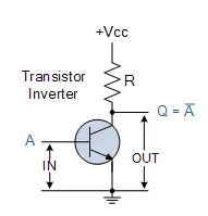
When the transistors base input at “A” is high, the transistor conducts and collector current flows producing a voltage drop across the resistor R thereby connecting the output point at “Q” to ground thus resulting in a zero voltage output at “Q“.
Likewise, when the transistors base input at “A” is low (0v), the transistor now switches “OFF” and no collector current flows through the resistor resulting in an output voltage at “Q” high at a value near to +Vcc.
Then, with an input voltage at “A” HIGH, the output at “Q” will be LOW and an input voltage at “A” LOW the resulting output voltage at “Q” is HIGH producing the complement or inversion of the input signal.
A standard Inverter or Logic NOT Gate, is usually made up from transistor switching circuits that do not switch from one state to the next instantly, there will always be some delay in the switching action.
Also as a transistor is a basic current amplifier, it can also operate in a linear mode and any small variation to its input level will cause a variation to its output level or may even switch “ON” and “OFF” several times if there is any noise present in the circuit. One way to overcome these problems is to use a Schmitt Inverter or Hex Inverter.
We know from the previous pages that all digital gates use only two logic voltage states and that these are generally referred to as Logic “1” and Logic “0” any TTL voltage input between 2.0v and 5v is recognised as a logic “1” and any voltage input below 0.8v is recognised as a logic “0” respectively.
A Schmitt Inverter is designed to operate or switch state when its input signal goes above an “Upper Threshold Voltage” or UTV limit in which case the output changes and goes “LOW”, and will remain in that state until the input signal falls below the “Lower Threshold Voltage” or LTV level in which case the output signal goes “HIGH”. In other words a Schmitt Inverter has some form of Hysteresis built into its switching circuit.
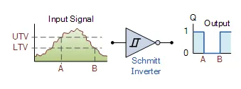
This switching action between an upper and lower threshold limit provides a much cleaner and faster “ON/OFF” switching output signal and makes the Schmitt inverter ideal for switching any slow-rising or slow-falling input signal and as such we can use a Schmitt trigger to convert these analogue signals into digital signals as shown.
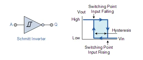
A very useful application of Schmitt inverters is when they are used as oscillators or sine-to-square wave converters for use as square wave clock signals.

The first circuit shows a very simple low power RC type oscillator using a Schmitt inverter to generate a square wave output waveform. Initially the capacitor C is fully discharged so the input to the inverter is “LOW” resulting in an inverted output which is “HIGH”. As the output from the inverter is fed back to its input and the capacitor via the resistor R the capacitor begins to charge up.
When the capacitors charging voltage reaches the upper threshold limit of the inverter, the inverter changes state, the output becomes “LOW” and the capacitor begins to discharge through the resistor until it reaches the lower threshold level were the inverter changes state again. This switching back and forth by the inverter produces a square wave output signal with a 33% duty cycle and whose frequency is given as: ƒ = 680/RC.
The second circuit converts a sine wave input (or any oscillating input for that matter) into a square wave output. The input to the inverter is connected to the junction of the potential divider network which is used to set the quiescent point of the circuit. The input capacitor blocks any DC component present in the input signal only allowing the sine wave signal to pass.
As this signal passes the upper and lower threshold points of the inverter the output also changes from “HIGH” to “LOW” and so on producing a square wave output waveform. This circuit produces an output pulse on the positive rising edge of the input waveform, but by connecting a second Schmitt inverter to the output of the first, the basic circuit can be modified to produce an output pulse on the negative falling edge of the input signal.
Commonly available logic NOT gate and Inverter IC’s include:

