Making a base wafer
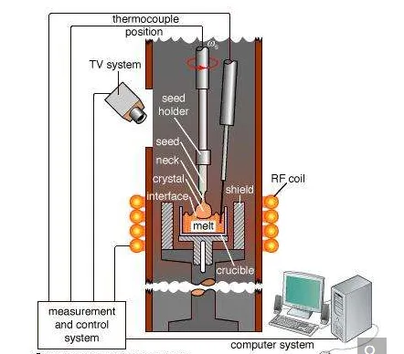
The substrate material, or base wafer, on which ICs are built is a semiconductor, such as silicon or gallium arsenide. In order to obtain consistent performance, the semiconductor must be extremely pure and a single crystal. The basic technique for creating large single crystals was discovered by the Polish chemist Jan Czochralski in 1916 and is now known as the Czochralski method. To create a single crystal of silicon by using the Czochralski method, electronic-grade silicon (refined to less than one part impurity in 100 billion) is heated to about 1,500 °C (2,700 °F) in a fused quartz crucible. Either an electron-donating element such as phosphorus or arsenic (for p-type semiconductors) or an electron-accepting element such as boron (for n-type semiconductors) is mixed in at a concentration of a few parts per billion. A small “seed” crystal, with a diameter of about 0.5 cm (0.2 inch) and a length of about 10 cm (4 inches), is attached to the end of a rod and lowered until it just penetrates the molten surface of the silicon. The rod and the crucible are then rotated in opposite directions while the rod is slowly withdrawn a few millimetres per second. Properly synchronized, these procedures result in the slow growth of a single crystal.
After many days the single crystal can be more than 1 metre (3.3 feet) in length and 300 mm (11.8 inches) in diameter. The large ingot is then sliced like a loaf of bread into thin wafers on which numerous ICs are fabricated simultaneously. The ICs are cut and separated after fabrication.
Building layers
All sorts of devices, such as diodes, transistors, capacitors, and resistors, can be built with p- and n-type semiconductors. It is convenient to be able to manufacture all of these different electronic components from the same few basic manufacturing steps.
ICs are made of layers, from about 0.000005 to 0.1 mm thick, that are built on the semiconductor substrate one layer at a time, with perhaps 30 or more layers in a final chip. Creating the different electrical components on a chip is a matter of outlining exactly where areas of n- and p-type are to be located on each layer. Each layer is etched, using lines and geometric shapes in the exact locations where the material is to be deposited.
A wafer can be changed in one of three fundamental ways: by deposition (that is, adding a layer), by etching or removing a layer, or by implantation (altering a layer’s composition). These processes are described below.