Bipolar transistors
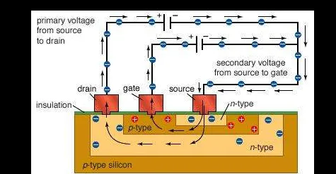
Bipolar transistors simultaneously use holes and electrons to conduct, hence their name (from “two polarities”). Like FETs, bipolar transistors contain p- and n-type materials configured in input, middle, and output regions. In bipolar transistors, however, these regions are referred to as the emitter, the base, and the collector. Instead of relying, as FETs do, on a secondary voltage source to change the polarity beneath the gate (the field effect), bipolar transistors use a secondary voltage source to provide enough energy for electrons to punch through the reverse-biased base-collector junction. As the electrons are energized, they jump into the collector and complete the circuit. Note that even with highly energetic electrons, the middle section of p-type material must be extremely thin for the electrons to pass through both junctions.

A bipolar base region can be fabricated that is much smaller than any CMOS transistor gate. This smaller size enables bipolar transistors to operate much faster than CMOS transistors. Bipolar transistors are typically used in applications where speed is very important, such as in radio-frequency ICs. On the other hand, although bipolar transistors are faster, FETs use less current. The type of switch a designer selects depends on which benefits are more important for the application: speed or power savings. This is one of many trade-off decisions engineers make in designing their circuits.