Basic Semiconductor Design
Any material can be classified as one of three types: conductor, insulator, or semiconductor. A conductor (such as copper or salt water) can easily conduct electricity because it has an abundance of free electrons. An insulator (such as ceramic or dry air) conducts electricity very poorly because it has few or no free electrons. A semiconductor (such as silicon or gallium arsenide) is somewhere between a conductor and an insulator. It is capable of conducting some electricity, but not much.
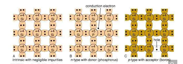
Doping silicon
Most ICs are made of silicon, which is abundant in ordinary beach sand. Pure crystalline silicon, as with other semiconducting materials, has a very high resistance to electrical current at normal room temperature. However, with the addition of certain impurities, known as dopants, the silicon can be made to conduct usable currents. In particular, the doped silicon can be used as a switch, turning current off and on as desired.
The process of introducing impurities is known as doping or implantation. Depending on a dopant’s atomic structure, the result of implantation will be either an n-type (negative) or a p-type (positive) semiconductor. An n-type semiconductor results from implanting dopant atoms that have more electrons in their outer (bonding) shell than silicon. The resulting semiconductor crystal contains excess, or free, electrons that are available for conducting current. A p-type semiconductor results from implanting dopant atoms that have fewer electrons in their outer shell than silicon. The resulting crystal contains “holes” in its bonding structure where electrons would normally be located. In essence, such holes can move through the crystal conducting positive charges.
The p-n junction
A p-type or an n-type semiconductor is not very useful on its own. However, joining these opposite materials creates what is called a p-njunction. A p-n junction forms a barrier to conduction between the materials. Although the electrons in the n-type material are attracted to the holes in the p-type material, the electrons are not normally energetic enough to overcome the intervening barrier. However, if additional energy is provided to the electrons in the n-type material, they will be capable of crossing the barrier into the p-type material—and current will flow. This additional energy can be supplied by applying a positive voltage to the p-type material. The negatively charged electrons will then be highly attracted to the positive voltage across the junction.
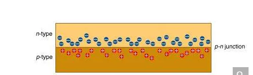
A p-n junction that conducts electricity when energy is added to the n material is called forward-biased because the electrons move forward into the holes. If voltage is applied in the opposite direction—a positive voltage connected to the n side of the junction—no current will flow. The electrons in the n material will still be attracted to the positive voltage, but the voltage will now be on the same side of the barrier as the electrons. In this state a junction is said to be reverse-biased. Since p-n junctions conduct electricity in only one direction, they are a type of diode. Diodes are essential building blocks of semiconductor switches.