Programmable Logic Devices
Programmable Logic Devices (PLDs) are the integrated circuits. They contain an array of AND gates & another array of OR gates. There are three kinds of PLDs based on the type of array(s), which has programmable feature.
The process of entering the information into these devices is known as programming. Basically, users can program these devices or ICs electrically in order to implement the Boolean functions based on the requirement. Here, the term programming refers to hardware programming but not software programming.
Programmable Read Only Memory (PROM)
Read Only Memory (ROM) is a memory device, which stores the binary information permanently. That means, we can’t change that stored information by any means later. If the ROM has programmable feature, then it is called as Programmable ROM (PROM). The user has the flexibility to program the binary information electrically once by using PROM programmer.
PROM is a programmable logic device that has fixed AND array & Programmable OR array. The block diagram of PROM is shown in the following figure.

Here, the inputs of AND gates are not of programmable type. So, we have to generate 2n product terms by using 2n AND gates having n inputs each. We can implement these product terms by using nx2n decoder. So, this decoder generates ‘n’ min terms.
Here, the inputs of OR gates are programmable. That means, we can program any number of required product terms, since all the outputs of AND gates are applied as inputs to each OR gate. Therefore, the outputs of PROM will be in the form of sum of min terms.
Example
Let us implement the following Boolean functions using PROM.
A(X,Y,Z)=∑m(5,6,7)A(X,Y,Z)=∑m(5,6,7)
B(X,Y,Z)=∑m(3,5,6,7)B(X,Y,Z)=∑m(3,5,6,7)
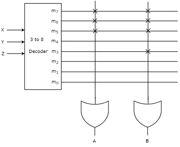
The given two functions are in sum of min terms form and each function is having three variables X, Y & Z. So, we require a 3 to 8 decoder and two programmable OR gates for producing these two functions. The corresponding PROM is shown in the following figure.

Here, 3 to 8 decoder generates eight min terms. The two programmable OR gates have the access of all these min terms. But, only the required min terms are programmed in order to produce the respective Boolean functions by each OR gate. The symbol ‘X’ is used for programmable connections.
Programmable Array Logic (PAL)
PAL is a programmable logic device that has Programmable AND array & fixed OR array. The advantage of PAL is that we can generate only the required product terms of Boolean function instead of generating all the min terms by using programmable AND gates. The block diagram of PAL is shown in the following figure.

Here, the inputs of AND gates are programmable. That means each AND gate has both normal and complemented inputs of variables. So, based on the requirement, we can program any of those inputs. So, we can generate only the required product terms by using these AND gates.
Here, the inputs of OR gates are not of programmable type. So, the number of inputs to each OR gate will be of fixed type. Hence, apply those required product terms to each OR gate as inputs. Therefore, the outputs of PAL will be in the form of sum of products form.
Example
Let us implement the following Boolean functions using PAL.
A=XY+XZ′A=XY+XZ′
A=XY′+YZ′A=XY′+YZ′
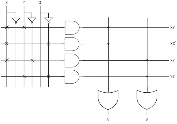
The given two functions are in sum of products form. There are two product terms present in each Boolean function. So, we require four programmable AND gates & two fixed OR gates for producing those two functions. The corresponding PAL is shown in the following figure.

The programmable AND gates have the access of both normal and complemented inputs of variables. In the above figure, the inputs X, X′X′, Y, Y′Y′, Z & Z′Z′, are available at the inputs of each AND gate. So, program only the required literals in order to generate one product term by each AND gate. The symbol ‘X’ is used for programmable connections.
Here, the inputs of OR gates are of fixed type. So, the necessary product terms are connected to inputs of each OR gate. So that the OR gates produce the respective Boolean functions. The symbol ‘.’ is used for fixed connections.
Programmable Logic Array (PLA)
PLA is a programmable logic device that has both Programmable AND array & Programmable OR array. Hence, it is the most flexible PLD. The block diagram of PLA is shown in the following figure.

Here, the inputs of AND gates are programmable. That means each AND gate has both normal and complemented inputs of variables. So, based on the requirement, we can program any of those inputs. So, we can generate only the required product terms by using these AND gates.
Here, the inputs of OR gates are also programmable. So, we can program any number of required product terms, since all the outputs of AND gates are applied as inputs to each OR gate. Therefore, the outputs of PAL will be in the form of sum of products form.
Example
Let us implement the following Boolean functions using PLA.
A=XY+XZ′A=XY+XZ′
B=XY′+YZ+XZ′B=XY′+YZ+XZ′
The given two functions are in sum of products form. The number of product terms present in the given Boolean functions A & B are two and three respectively. One product term, Z′XZ′X is common in each function.
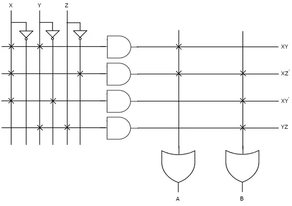
So, we require four programmable AND gates & two programmable OR gates for producing those two functions. The corresponding PLA is shown in the following figure.

The programmable AND gates have the access of both normal and complemented inputs of variables. In the above figure, the inputs X, X′X′, Y, Y′Y′, Z & Z′Z′, are available at the inputs of each AND gate. So, program only the required literals in order to generate one product term by each AND gate.
All these product terms are available at the inputs of each programmable OR gate. But, only program the required product terms in order to produce the respective Boolean functions by each OR gate. The symbol ‘X’ is used for programmable connections.