DESIGN OF COMBINATIONAL CIRCUIT
Design of a combinational circuit starts from the outline of the problem and ends in a logic circuit diagram.
1. State the given problems completely and exactly.
2. Interpret the problem to determine available input and required output variables.
3. Assign a letter symbol to each input variable and each output variable.
4. Design a truth table that defines the required relations between inputs and outputs.
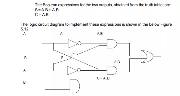
5. Obtain the simplified Boolean expression for each output
6. Draw a logic circuit diagram to implement the Boolean expression. The design procedure is illustrated below with the design of adder circuits because addition is the most basic arithmetic operation for any computer system.
The following four rules summarize additionin binary number system.
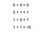
The first three operations produce a single-digit sum, but when both augends and addend bits are equal to 1, the sum consists of two digits. The higher significant bit of this result is called a carry. When both augends and addend numbers contain more than one digit, the carry obtainedfrom addition of two bits at any stage is added to the next pair of significant bits. A combinational circuit that performs the addition of two bits is called a half-adder. One that performs the addition of three bits (two significant bits and previous carry) is called a full-adder. The name of the former comes from that fact that two half-adders can be employed to implement of a fulladder.
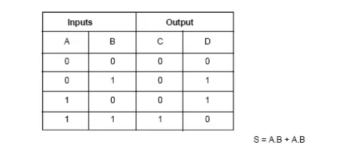
Design of Half-Adder
From the definition given above, a half-adder needs two binary inputs and two binary outputs. The input variables designate the augends and addend bits whereas the output variables and addend bits whereas the output variables produce the sum and carry bits. Let A and B be the two inputs and S (for sum) and C (for carry) be the two outputs. The truth table of the Figure defines the function of a half-adder.