Bipolar Junction Transistors (BJT)
The invention of the bipolar transistor in 1948 ushered in a revolution in electronics. Technical feats previously requiring relatively large, mechanically fragile, power-hungry vacuum tubes were suddenly achievable with tiny, mechanically rugged, power-thrifty specks of crystalline silicon. This revolution made possible the design and manufacture of lightweight, inexpensive electronic devices that we now take for granted. Understanding how transistors function is of paramount importance to anyone interested in understanding modern electronics.
The Function and Applications for Bipolar Junction Transistors
My intent here is to focus as exclusively as possible on the practical function and application of bipolar transistors, rather than to explore the quantum world of semiconductor theory. Discussions of holes and electrons are better left to another chapter in my opinion. Here I want to explore how to use these components, not analyze their intimate internal details. I don’t mean to downplay the importance of understanding semiconductor physics, but sometimes an intense focus on solid-state physics detracts from understanding these devices’ functions on a component level. In taking this approach, however, I assume that the reader possesses a certain minimum knowledge of semiconductors: the difference between “P” and “N” doped semiconductors, the functional characteristics of a PN (diode) junction, and the meanings of the terms “reverse biased” and “forward biased.” If these concepts are unclear to you, it is best to refer to earlier chapters in this book before proceeding with this one.
BJT Layers
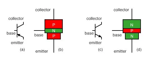
A bipolar transistor consists of a three-layer “sandwich” of doped (extrinsic) semiconductor materials, (a and c) either P-N-P or N-P-N (b and c ). Each layer forming the transistor has a specific name, and each layer is provided with a wire contact for connection to a circuit. The schematic symbols are shown in the figure (a) and (c).

BJT transistor: (a) PNP schematic symbol, (b) layout (c) NPN schematic symbol, (d) layout.
The functional difference between a PNP transistor and an NPN transistor is the proper biasing (polarity) of the junctions when operating.
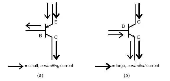
Bipolar transistors work as current-controlled current regulators. In other words, transistors restrict the amount of current passed according to a smaller, controlling current. The main current that is controlled goes from collector to emitter, or from emitter to collector, depending on the type of transistor it is (NPN or PNP, respectively). The small current that controls the main current goes from base to emitter, or from emitter to base, once again depending on the kind of transistor it is (NPN or PNP, respectively). According to the standards of semiconductor symbology, the arrow always points in the direction of current flow.

The direction of the small, controlling current and the large controlled current for (a) a PNP and (b) an NPN transistor.
Bipolar Transistors Contain Two Types of Semiconductor Material
Bipolar transistors are called bipolar because the main flow of current through them takes place in two types of semiconductor material: P and N, as the main current goes from emitter to collector (or vice versa). In other words, two types of charge carriers—electrons and holes—comprise this main current through the transistor.
As you can see, the controlling current and the controlled current always mesh together through the emitter wire, and their currents flow in the direction of the transistor’s arrow. This is the first and foremost rule in the use of transistors: all currents must be going in the proper directions for the device to work as a current regulator. The small, controlling current is usually referred to simply as the base current because it is the only current that goes through the base wire of the transistor. Conversely, the large, controlled current is referred to as the collector current because it is the only current that goes through the collector wire. The emitter current is the sum of the base and collector currents, in compliance with Kirchhoff’s Current Law.
No current through the base of the transistor shuts the transistor off like an open switch and prevents current through the collector. A base current turns the transistor on like a closed switch and allows a proportional amount of current through the collector. Collector current is primarily limited by the base current, regardless of the amount of voltage available to push it. The next section will explore in more detail the use of bipolar transistors as switching elements.