Forward Bias and Reverse Bias
A forward-biased diode conducts current and drops a small voltage across it, leaving most of the battery voltage dropped across the lamp. If the battery’s polarity is reversed, the diode becomes reverse-biased, and drops all of the battery’s voltage leaving none for the lamp. If we consider the diode to be a self-actuating switch (closed in the forward-bias mode and open in the reverse-bias mode), this behavior makes sense. The most substantial difference is that the diode drops a lot more voltage when conducting than the average mechanical switch (0.7 volts versus tens of millivolts).
This forward-bias voltage drop exhibited by the diode is due to the action of the depletion region formed by the P-N junction under the influence of an applied voltage. If no voltage applied is across a semiconductor diode, a thin depletion region exists around the region of the P-N junction, preventing current flow. (Figure below (a)) The depletion region is almost devoid of available charge carriers, and acts as an insulator:
Diode representations: PN-junction model, schematic symbol, physical part.
The schematic symbol of the diode is shown in the figure above (b) such that the anode (pointing end) corresponds to the P-type semiconductor at (a). The cathode bar, non-pointing end, at (b) corresponds to the N-type material at (a). Also note that the cathode stripe on the physical part (c) corresponds to the cathode on the symbol.
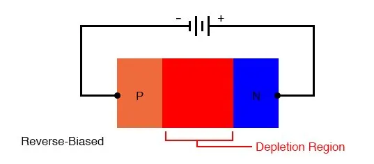
Reverse Bias Diode Configuration
If a reverse-biasing voltage is applied across the P-N junction, this depletion region expands, further resisting any current through it. (Figure below)
Depletion region expands with reverse bias.
Conversely, if a forward-biasing voltage is applied across the P-N junction, the depletion region collapses becoming thinner. The diode becomes less resistive to current through it. In order for a sustained current to go through the diode; though, the depletion region must be fully collapsed by the applied voltage. This takes a certain minimum voltage to accomplish, called the forward voltage as illustrated in the figure below.
Increasing forward bias from (a) to (b) decreases depletion region thickness.
For silicon diodes, the typical forward voltage is 0.7 volts, nominal. For germanium diodes, the forward voltage is only 0.3 volts. The chemical constituency of the P-N junction comprising the diode accounts for its nominal forward voltage figure, which is why silicon and germanium diodes have such different forward voltages. Forward voltage drop remains approximately constant for a wide range of diode currents, meaning that diode voltage drop is not like that of a resistor or even a normal (closed) switch. For most simplified circuit analysis, the voltage drop across a conducting diode may be considered constant at the nominal figure and not related to the amount of current.