555 Timer
The 555 Timer IC got its name from the three 5KΩ5KΩ resistors that are used in its voltage divider network. This IC is useful for generating accurate time delays and oscillations. This chapter explains about 555 Timer in detail.
In this section, first let us discuss about the pin diagram of 555 Timer IC and then its functional diagram.
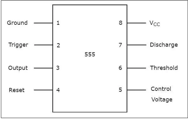
The 555 Timer IC is an 8 pin mini Dual-Inline Package (DIP). The pin diagram of a 555 Timer IC is shown in the following figure −
The significance of each pin is self-explanatory from the above diagram. This 555 Timer IC can be operated with a DC supply of +5V to +18V. It is mainly useful for generating non-sinusoidal wave forms like square, ramp, pulse & etc
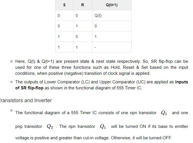
The pictorial representation showing the internal details of a 555 Timer is known as functional diagram.
The functional diagram of 555 Timer IC is shown in the following figure −
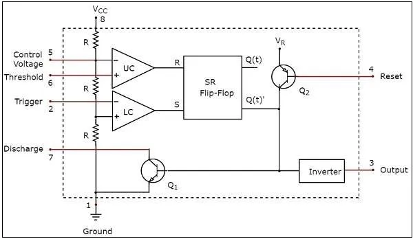
Observe that the functional diagram of 555 Timer contains a voltage divider network, two comparators, one SR flip-flop, two transistors and an inverter. This section discusses about the purpose of each block or component in detail −