Window Comparator
A Window Comparator is basically the inverting and the non-inverting comparators above combined into a single comparator stage. The window comparator detects input voltage levels that are within a specific band or window of voltages, instead of indicating whether a voltage is greater or less than some preset or fixed voltage reference point.
This time, instead of having just one reference voltage value, a window comparator will have two reference voltages implemented by a pair of voltage comparators. One which triggers an op-amp comparator on detection of some upper voltage threshold, VREF(UPPER) and one which triggers an op-amp comparator on detection of a lower voltage threshold level, VREF(LOWER). Then the voltage levels between these two upper and lower reference voltages is called the “window”, hence its name.
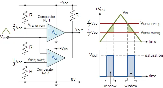
Using our idea above of a voltage divider network, if we now use three equal value resistors so that R1 = R2 = R3 = R we can create a very simple window comparator circuit as shown. Also as the resistive values are all equal, the voltage drops across each resistor will also be equal at one-third the supply voltage, 1/3Vcc. Then in this simple example, we can set the upper reference voltage to 2/3Vcc and the lower reference voltage to 1/3Vcc. Consider the window comparator circuit below.
Window Comparator Circuit
When VIN is below the lower voltage level, VREF(LOWER) which equates to 1/3Vcc, the output will be LOW. When VIN exceeds this 1/3Vcc lower voltage level, the first op-amp comparator detects this and switches the output HIGH to Vcc.
As VIN continues to increase it passes the upper voltage level, VREF(UPPER) at 2/3Vcc and the second op-amp comparator detects this and switches the output back LOW. Then the difference between VREF(UPPER) and VREF(LOWER) (which is 2/3Vccc – 1/3Vcc in this example) creates the switching window for the positive going signal.
Lets now assume that VIN is at its maximum value and equal to Vcc. As VIN decreases it passes the upper voltage level VREF(UPPER) of the second op-amp comparator which switches the output HIGH. As VIN continues to decrease it passes the lower voltage level, VREF(LOWER) of the first op-amp comparator once again switching the output LOW.
Then the difference between VREF(UPPER) and VREF(LOWER) creates the window for the negative going signal. So we can see that as VIN passes above or passes below the upper and lower reference levels set by the two op-amp comparators, the output signal VOUT will be HIGH or LOW.
In this simple example we have set the upper trip level at 2/3Vcc and the lower trip level at 1/3Vcc (because we used three equal value resistors), but can be any values we choose by adjusting the input thresholds. As a result, the window width can be customized for a given application.
If we used a dual power supply and set the upper and lower trip levels to say ±10 volts and VIN was a sinusoidal waveform, then we could use this window comparator circuit as a zero crossing detector of the sine wave which would produce an output, HIGH or LOW every time the sine wave crossed the zero volts line from positive to negative or negative to positive.
We can take this idea of detecting voltage levels further by connecting a number of different op-amp comparators together with them all using a common input signal, but with each comparator using a different reference voltage set by our now familiar voltage divider network across the supply. Consider the voltage level detector circuit below.
Comparator Voltage Level Detector
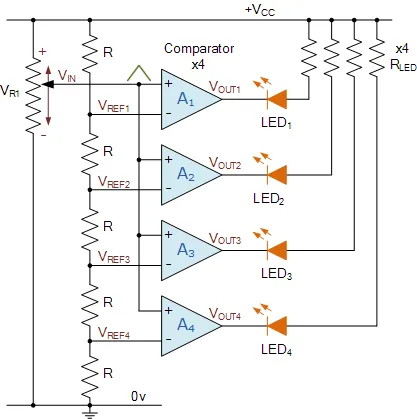
As above, the voltage divider network provides a set of reference voltages for the individual op-amp comparator circuits. To produce the four reference voltages will require five resistors. The junction at the bottom pair of resistors will produce a reference voltage that is one-fifth the supply voltage, 1/5Vcc using equal value resistors. The second pair 2/5Vcc, a third pair 3/5Vcc and so on, with these reference voltages increasing by a fixed amount of one-fifth (1/5) towards 5/5Vcc which is actually Vcc.
As the common input voltage increases, the output of each op-amp comparator circuit switches in turn thereby turning OFF the connected LED starting with the lower comparator, A4 and upwards towards A1 as the input voltage increases. So by setting the values of the resistors in the voltage divider network, the comparators can be configured to detect any voltage level. One good example of the use of voltage level detection and indication would be for a battery condition monitor by reversing the LED’s and connecting them to 0V (ground) instead of VCC.
Also by increasing the number of op-amp comparators in the set, more trigger points can be created. So for example, if we had eight op-amp comparators in the chain and fed the output of each comparator to an 8-to-3 line Digital Encoder, we could make a very simple analogue-to-digital converter, (ADC) that would convert the analogue input signal into a 3-bit binary code (0-to-7).
Op-amp Comparator with Positive Feedback
We have seen here that operational amplifiers can be configured to operate as comparators in their open-loop mode, and this is fine if the input signal varies rapidly or is not too noisy. However if the input signal, VIN is slow to change or electrical noise is present, then the op-amp comparator may oscillate switching its output back and forth between the two saturation states, +Vcc and -Vcc as the input signal hovers around the reference voltage, VREF level. One way to overcome this problem and to avoid the op-amp from oscillating is to provide positive feedback around the comparator.
As its name implies, positive feedback is a technique for feeding back a part or fraction of the output signal that is in phase to the non-inverting input of the op-amp via a potential divider set up by two resistors with the amount of feedback being proportional to their ratio.
The use of positive feedback around an op-amp comparator means that once the output is triggered into saturation at either level, there must be a significant change to the input signal VIN before the output switches back to the original saturation point. This difference between the two switching points is called hysteresis producing what is commonly called a Schmitt trigger circuit. Consider the inverting comparator circuit below.
Inverting Op-amp Comparator with Hysteresis
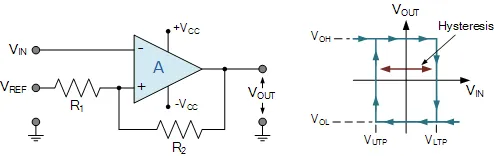
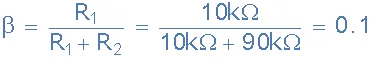
For the inverting comparator circuit above, VIN is applied to the inverting input of the op-amp. Resistors R1 and R2 form a voltage divider network across the comparator providing the positive feedback with part of the output voltage appearing at the non-inverting input. The amount of feedback is determined by the resistive ratio of the two resistors used and which is given as:
Voltage Divider Equation

Where: β (beta) can be used to indicate the feedback fraction.
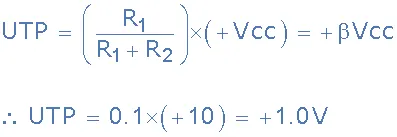
When the input signal is less than the reference voltage, VIN < VREF, the output voltage will be HIGH, VOH and equal to the positive saturation voltage. As the output is HIGH and positive, the value of the reference voltage on the non-inverting input will be approximately equal to: +β*Vcc called the Upper Trip Point or UTP.
As the input signal, VIN increases it becomes equal too this upper trip point voltage, VUTP level at the non-inverting input. This causes the comparators output to change state becoming LOW, VOL and equal to the negative saturation voltage as before.
But the difference this time is that a second trip point voltage value is created because a negative voltage now appears at the non-inverting input which is equal to: -β*Vcc as a result of the negative saturation voltage at the output. Then the input signal must now fall below this second voltage level, called the Lower Trip Point or LTP for the voltage comparators output to change or switch back to its original positive state.
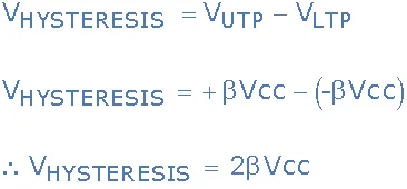
So we can see that when the output changes state, the reference voltage at the non-inverting input also changes creating two different reference voltage values and two different switching points. One called the Lower Upper Trip Point (UTP) and the other being called the Lower Trip Point (LTP). The difference between these two trip points is called Hysteresis.
The amount of hysteresis is determined by the feedback fraction, β of the output voltage fed back to the non-inverting input. The advantage of positive feedback is that the resulting comparator Schmitt trigger circuit is immune to erratic triggering caused by noise or slowly changing input signals within the hysteresis band producing a cleaner output signal as the op-amp comparators output is only triggered once.
So for positive output voltages, VREF = +β*Vcc, but for negative output voltages, VREF = -β*Vcc. Then we can say that the amount of voltage hysteresis will be given as:
We can also produce a non-inverting op-amp comparator circuit with built in hysteresis by changing the input and reference terminals as shown:
Non-inverting Op-amp Comparator with Hysteresis
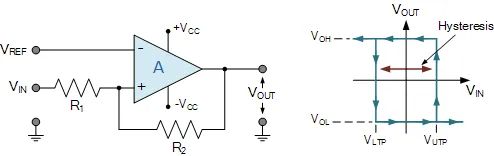
Note that the arrows on the hysteresis graph indicate the direction of switching at the upper and lower trip points.
Comparator Example No1
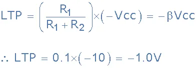
An operational amplifier is to be used with positive feedback to produce a Schmitt trigger circuit. If resistor, R1 = 10kΩ and resistor, R2 = 90kΩ, what will be the values of the upper and lower switching points of the reference voltage and the width of the hysteresis if the op-amp is connected to a dual ±10v power supply.
Given: R1 = 10kΩ, R2 = 90kΩ. Power supply +Vcc = 10v and -Vcc = 10v.
Feedback Fraction:
Upper Voltage Trip Point, VUTP
Lower Voltage Trip Point, VLTP
Hysteresis width:
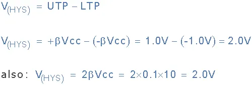
Then the reference voltage VREF, switches between +1V and -1V as the output saturates from one level to the other. Hopefully we can see from this simple example that the width of this hysteresis, 2 volts in total, can be made larger or smaller simply by adjusting the voltage divider ratio of the feedback resistors R1 and R2.