Astable Multivibrator Circuits
Astable Multivibrators are the most commonly used type of multivibrator circuit. An astable multivibrator is a free running oscillator that have no permanent “meta” or “steady” state but are continually changing there output from one state (LOW) to the other state (HIGH) and then back again. This continual switching action from “HIGH” to “LOW” and “LOW” to “HIGH” produces a continuous and stable square wave output that switches abruptly between the two logic levels making it ideal for timing and clock pulse applications.
As with the previous monostable multivibrator circuit above, the timing cycle is determined by the RC time constant of the resistor-capacitor, RC Network. Then the output frequency can be varied by changing the value(s) of the resistors and capacitor in the circuit.
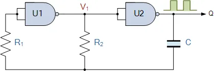
NAND Gate Astable Multivibrator
The astable multivibrator circuit uses two CMOS NOT gates such as the CD4069 or the 74HC04 hex inverter ICs, or as in our simple circuit below a pair of CMOS NAND such as the CD4011 or the 74LS132 and an RC timing network. The two NAND gates are connected as inverting NOT gates.
Suppose that initially the output from the NAND gate U2 is HIGH at logic level “1”, then the input must therefore be LOW at logic level “0” (NAND gate principles) as will be the output from the first NAND gate U1. Capacitor, C is connected between the output of the second NAND gate U2 and its input via the timing resistor, R2. The capacitor now charges up at a rate determined by the time constant of R2 and C.
As the capacitor, C charges up, the junction between the resistor R2 and the capacitor, C, which is also connected to the input of the NAND gate U1 via the stabilizing resistor, R2 decreases until the lower threshold value of U1 is reached at which point U1 changes state and the output of U1 now becomes HIGH. This causes NAND gate U2 to also change state as its input has now changed from logic “0” to logic “1” resulting in the output of NAND gate U2 becoming LOW, logic level “0”.
Capacitor C is now reverse biased and discharges itself through the input of NAND gate U1. Capacitor, C charges up again in the opposite direction determined by the time constant of both R2 and C as before until it reaches the upper threshold value of NAND gate U1. This causes U1 to change state and the cycle repeats itself over again.
Then, the time constant for a NAND gate Astable Multivibrator is given as T = 2.2RC in seconds with the output frequency given as ƒ = 1/T.
For example: if the resistor R2 = 10kΩ and the capacitor C = 45nF, the oscillation frequency of the circuit would be given as:
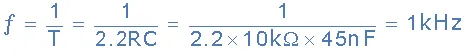
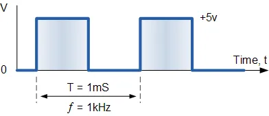
Then the output frequency is calculated as being 1kHz, which equates to a time constant of 1ms so the output waveform would look like:
Bistable Multivibrator Circuits
The Bistable Multivibrators circuit is basically a SR flip-flop that we look at in the previous tutorials with the addition of an inverter or NOT gate to provide the necessary switching function. As with flip-flops, both states of a bistable multivibrator are stable, and the circuit will remain in either state indefinitely. This type of multivibrator circuit passes from one state to the other “only” when a suitable external trigger pulse T is applied and to go through a full “SET-RESET” cycle two triggering pulses are required. This type of circuit is also known as a “Bistable Latch”, “Toggle Latch” or simply “T-latch”.
NAND Gate Bistable Multivibrator
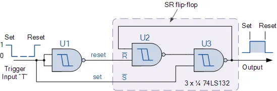
The simplest way to make a Bistable Latch is to connect together a pair of Schmitt NAND gates to form a SR latch as shown above. The two NAND gates, U2 and U3 form the bistable which is triggered by the input NAND gate, U1. This U1 NAND gate can be omitted and replaced by a single toggle switch to make a switch debounce circuit as seen previously in the SR Flip-flop tutorial.
When the input pulse goes “LOW” the bistable latches into its “SET” state, with its output at logic level “1”, until the input goes “HIGH” causing the bistable to latch into its “RESET” state, with its output at logic level “0”. The output of a bistable multivibrator will stay in this “RESET” state until another input pulse is applied and the whole sequence will start again.
Then a Bistable Latch or “Toggle Latch” is a two-state device in which both states either positive or negative, (logic “1” or logic “0”) are stable.
Bistable Multivibrators have many applications such as frequency dividers, counters or as a storage device in computer memories but they are best used in circuits such as Latches and Counters.
555 Timer Circuit.
Simple Monostable or Astable multivibrators can now be easily made using standard commonly available waveform generator IC’s specially design to create timing and oscillator circuits. Relaxation oscillators can be constructed simply by connecting a few passive components to their input pins with the most commonly used waveform generator type IC being the classic 555 timer.
The 555 Timer is a very versatile low cost timing IC that can produce a very accurate timing periods with good stability of around 1% and which has a variable timing period from between a few micro-seconds to many hours with the timing period being controlled by a single RC network connected to a single positive supply of between 4.5 and 16 volts.
The NE555 timer and its successors, ICM7555, CMOS LM1455, DUAL NE556 etc, are covered in the 555 Oscillator tutorial and other good electronics based websites, so are only included here for reference purposes as a clock pulse generator. The 555 connected as an Astable Multivibrator is shown below.
NE555 Astable Multivibrator
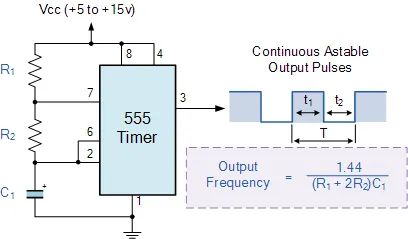
Here the 555 timer is connected as a basic Astable Multivibrator producing a continuous output waveform. Pins 2 and 6 are connected together so that it will re-trigger itself on each timing cycle, thereby functioning as an Astable oscillator. Capacitor, C1 charges up through resistor, R1 and resistor, R2 but discharges only through resistor, R2 as the other side of R2 is connected to the discharge terminal, pin 7. Then the timing period of t1 and t2 is given as:
· t1 = 0.693 (R1 + R2) C1
· t2 = 0.693 (R2) C1
· T = t1 + t2 = 0.693 (R1 + 2R2) C1
The voltage across the capacitor, C1 ranges from between 1/3 Vcc to approximately 2/3 Vcc depending upon the RC timing period. This type of circuit is very stable as it operates from a single supply rail resulting in an oscillation frequency which is independent of the supply voltage Vcc.
In the next tutorial about Sequential Logic Circuits, we will look another type of clock controlled flop-flop called a Data Latch. Data latches are very useful sequential circuits which can be made from any standard gated SR flip-flop and used for frequency division to produce various ripple counters, frequency dividers and latches.