Monostable Multivibrator Circuits
Monostable Multivibrators or “one-shot” pulse generators are generally used to convert short sharp pulses into wider ones for timing applications. Monostable multivibrators generate a single output pulse, either “HIGH” or “LOW”, when a suitable external trigger signal or pulse T is applied.
This trigger pulse signal initiates a timing cycle which causes the output of the monostable to change state at the start of the timing cycle, ( t1 ) and remain in this second state until the end of the timing period, ( t2 ) which is determined by the time constant of the timing capacitor, CT and the resistor, RT.
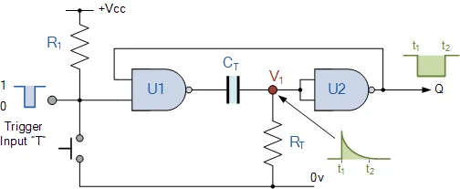
The monostable multivibrator now stays in this second timing state until the end of the RC time constant and automatically resets or returns itself back to its original (stable) state. Then, a monostable circuit has only one stable state. A more common name for this type of circuit is simply a “Flip-Flop” as it can be made from two cross-coupled NAND gates (or NOR gates) as we have seen previously. Consider the circuit below.
Simple NAND Gate Monostable Circuit

Suppose that initially the trigger input T is held HIGH at logic level “1” by the resistor R1 so that the output from the first NAND gate U1 is LOW at logic level “0”, (NAND gate principals). The timing resistor, RT is connected to a voltage level equal to logic level “0”, which will cause the capacitor, CT to be discharged. The output of U1 is LOW, timing capacitor CT is completely discharged therefore junction V1 is also equal to “0” resulting in the output from the second NAND gate U2, which is connected as an inverting NOT gate will therefore be HIGH.
The output from the second NAND gate, ( U2 ) is fed back to one input of U1 to provide the necessary positive feedback. Since the junction V1 and the output of U1 are both at logic “0” no current flows in the capacitor CT. This results in the circuit being Stable and it will remain in this state until the trigger input T changes.
If a negative pulse is now applied either externally or by the action of the push-button to the trigger input of the NAND gate U1, the output of U1 will go HIGH to logic “1” (NAND gate principles).
Since the voltage across the capacitor cannot change instantaneously (capacitor charging principals) this will cause the junction at V1 and also the input to U2 to also go HIGH, which in turn will make the output of the NAND gate U2 change LOW to logic “0” The circuit will now remain in this second state even if the trigger input pulse T is removed. This is known as the Meta-stable state.
The voltage across the capacitor will now increase as the capacitor CT starts to charge up from the output of U1 at a time constant determined by the resistor/capacitor combination. This charging process continues until the charging current is unable to hold the input of U2 and therefore junction V1 HIGH.
When this happens, the output of U2 switches HIGH again, logic “1”, which in turn causes the output of U1 to go LOW and the capacitor discharges into the output of U1 under the influence of resistor RT. The circuit has now switched back to its original stable state.
Thus for each negative going trigger pulse, the monostable multivibrator circuit produces a LOW going output pulse. The length of the output time period is determined by the capacitor/resistor combination (RC Network) and is given as the Time Constant T = 0.69RC of the circuit in seconds. Since the input impedance of the NAND gates is very high, large timing periods can be achieved.
As well as the NAND gate monostable type circuit above, it is also possible to build simple monostable timing circuits that start their timing sequence from the rising-edge of the trigger pulse using NOT gates, NAND gates and NOR gates connected as inverters as shown below.
NOT Gate Monostable Multivibrator

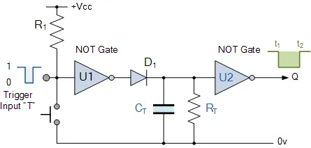
As with the NAND gate circuit above, initially the trigger input T is HIGH at a logic level “1” so that the output from the first NOT gate U1 is LOW at logic level “0”. The timing resistor, RT and the capacitor, CT are connected together in parallel and also to the input of the second NOT gate U2. As the input to U2 is LOW at logic “0” its output at Q is HIGH at logic “1”.
When a logic level “0” pulse is applied to the trigger input T of the first NOT gate it changes state and produces a logic level “1” output. The diode D1 passes this logic “1” voltage level to the RC timing network. The voltage across the capacitor, CT increases rapidly to this new voltage level, which is also connected to the input of the second NOT gate. This in turn outputs a logic “0” at Q and the circuit stays in this Meta-stable state as long as the trigger input T applied to the circuit remains LOW.
When the trigger signal returns HIGH, the output from the first NOT gate goes LOW to logic “0” (NOT gate principals) and the fully charged capacitor, CT starts to discharge itself through the parallel resistor, RT connected across it. When the voltage across the capacitor drops below the lower threshold value of the input to the second NOT gate, its output switches back again producing a logic level “1” at Q. The diode D1 prevents the timing capacitor from discharging itself back through the first NOT gates output.
Then, the Time Constant for a NOT gate Monostable Multivibrator is given as T = 0.8RC + Trigger in seconds.
One main disadvantage of Monostable Multivibrators is that the time between the application of the next trigger pulse T has to be greater than the RC time constant of the circuit.